Market Overview
The global CMP Slurry Market is projected to be valued at USD 13.3 billion by the end of 2025 and is further expected to reach a market value of USD 44.0 billion in 2034 at a CAGR of 14.2%.
ℹ
To learn more about this report –
Download Your Free Sample Report Here
The global CMP slurry market comes under the wide category of the semiconductor manufacturing business, which itself is technologically growing a lot. CMP slurry is an agent that plays an important role during the process of planarization, giving a regular and smooth finish to the semiconductor wafer with accuracy in the photolithography process. The market has experienced a very healthy growth path arising from increasing demand for sophisticated semiconductors and support from technologies related to 5G networks, IOT devices, and applications driven by artificial intelligence.
Applications related to CMP slurries have occurred in three principal areas: oxide polishing, metal polishing, and dielectric polishing; of these types, silica-based slurries take the greater percentage of market shares due to versatility and cost-effectiveness, while ceria-based slurries are gaining traction for higher precision requirements across niche applications.
Fast miniaturization of the electronic components and migration to the higher nodes are some of the two major emerging trends in the CMP slurry market. The leading chip manufacturers are continuously investing in the invention of new formulation slurries, meeting unique requirements posed by advanced semiconductor devices. Furthermore, the increasing infiltration of 3D NAND and FinFET architectures has accelerated the demand for CMP slurries tailored to meet the complex layers of modern chips. This innovation-driven trend is further complemented by the expansion of semiconductor fabs, especially in Asia-Pacific, now the epicenter of global chip production.
Even with the attractive growth prospects presented, there are certain obstacles, mainly from the high expense in R and D and firm performance requirements across the value chain. The kind of formulation followed to make a slurry for polishing at CMP in most cases should not scratch either or introduce possible defects to the work surface. Much research and expenses in development mean big investment, normally a barrier that few players can climb easily.
Also, because the semiconductor industry is cyclic and further prone to geopolitical conflicts, disruption in supply chains and alterations in market conditions could result. Advancement in recycling and reusing slurries stands to present an opportunity for attaining sustainability coupled with a reduction in production cost.
The maximum share comes from the Asia-Pacific region, which is dominated by countries such as China, Taiwan, and South Korea. The leading position is held by this region due to its leadership in semiconductor manufacturing. North America and Europe follow their contribution with their emphasis on high-performance computing and automotive electronics. In the emerging markets, however, demand for advanced CMP slurries is growing, gradually showing a wide area of virgin potential.
The CMP slurry market is likely to benefit in the coming years from several new opportunities that have emerged across industries. The arrival of electric vehicles and autonomous driving raised the stakes for semiconductor component reliability and performance. Similarly, renewable energy systems, such as solar panels and energy storage devices, are proliferating, which again raises the need for CMP processes to enhance efficiency.
The CMP slurry market, poised in the wake of an increased focus on digital transformation and technological innovation at a global scale, is continuously presenting growth, though with certain challenges that may require strategic solutions by participants.
The US CMP Slurry Market
The US CMP Slurry Market is projected to reach USD 1.7 billion in 2025 at a compound annual growth rate of 7.0% over its forecast period.
The United States CMP slurry market is very significant in the global semiconductor industry, with a robust technological infrastructure, extensive R&D capabilities, and a skilled workforce. With giants like Intel, NVIDIA, and AMD, the U.S. is the hotbed of semiconductor innovation that keeps pushing the demand for high-performance CMP slurries needed for advanced chip fabrication. The U.S. The CMP slurry market reflects a stable growth pattern on the back of advanced chip manufacturing processes, integration of AI, and the rapid expansion of 5G technology.
The demographic dividend that the U.S. market represents includes a good balance of an educated workforce combined with heavy investment in the field of STEM. Besides, the intent for innovation has been further crystalized with focused government initiatives in the form of the CHIPS and Science Act, which aims to address the domestic production of semiconductors in the country. This has led to huge funding, infrastructure development, and partnering of slurry manufacturers with semiconductor fabs for collaboration on stringent next-generation technologies.
This is a resilient market that continues to be robust despite the vulnerabilities in supply chains and the high cost of R&D. These are challenges that could be overcome through the localization of supply chains and the development of sustainable slurry solutions. Furthermore, emerging technologies such as autonomous vehicles and IoT devices are expected to spur demand for advanced CMP slurries. With the technological edge, supportive policies, and skilled workforce, the U.S. is well-positioned to continue leading in the CMP slurry market to maintain competitiveness in the rapidly changing semiconductor landscape.
Key Takeaways
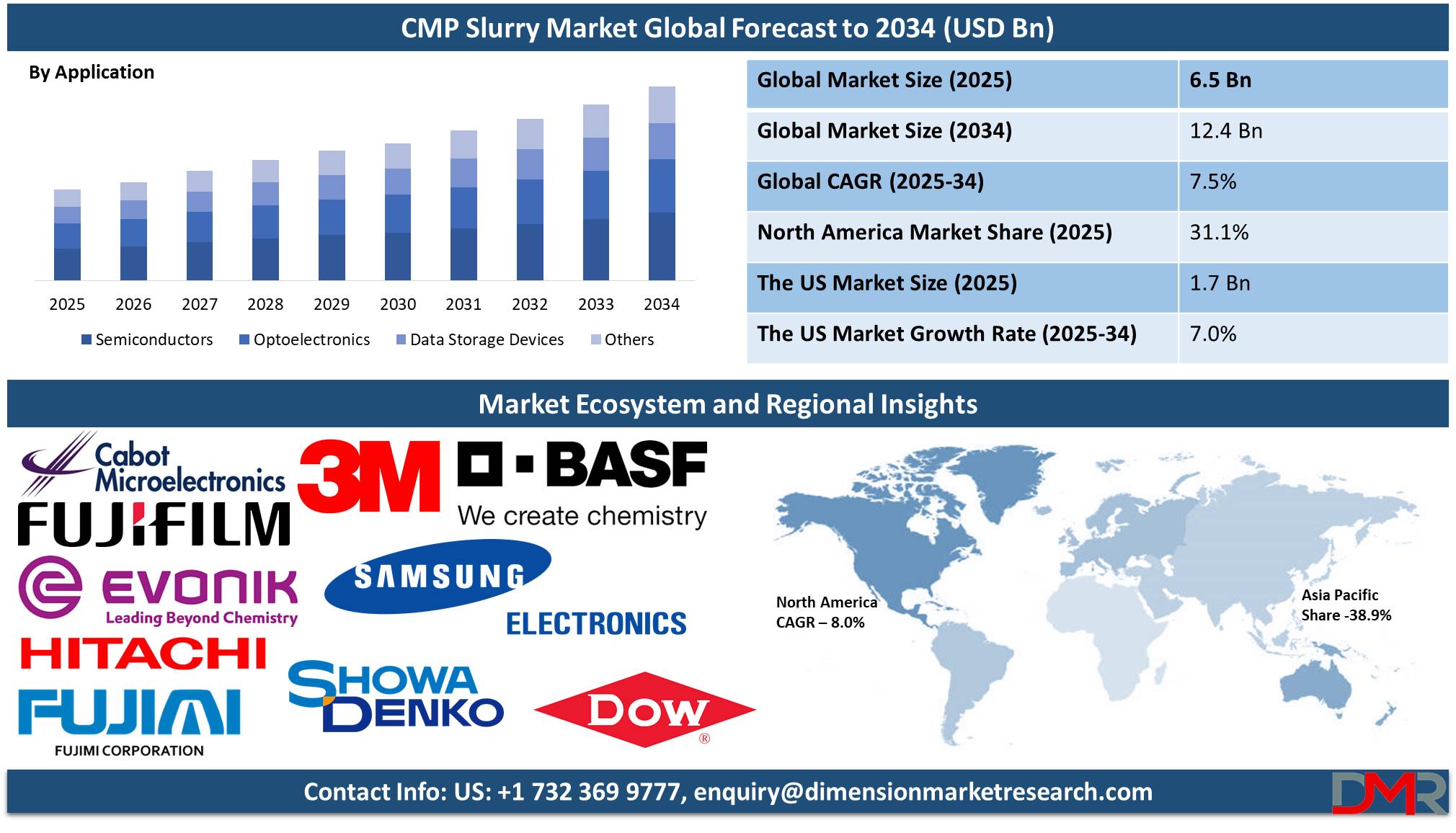
- Global Market Value: The Global CMP Slurry Market size is estimated to have a value of USD 6.5 billion in 2025 and is expected to reach USD 12.4 billion by the end of 2034.
- The US Market Value: The US CMP Slurry Market is projected to be valued at USD 1.7 billion in 2025. It is expected to witness subsequent growth in the upcoming period as it holds USD 3.1 billion in 2034 at a CAGR of 13.3%.
- Regional Analysis: Asia Pacific is expected to have the largest market share in the Global CMP Slurry Market with a share of about 38.9% in 2025.
- Key Players: Some of the major key players in the Global CMP Slurry Market are Cabot Microelectronics Corporation, FUJIFILM Holdings Corporation, Hitachi Ltd., Samsung Electronics Co., Ltd., The Dow Chemical Company, and many others.
- Global Growth Rate: The market is growing at a CAGR of 7.5 percent over the forecasted period.
Use Cases
- Semiconductor Wafers: CMP slurries for the planarization of silicon wafers are a main process in integrated circuit manufacturing; such a smooth and flat resultant surface is required for eventual photolithographic steps. Also, this develops the requirement during manufacturing for higher nodes such as 5 nm and 3 nm chips to have low defects and high selectivity, demanding strict state-of-the-art CMP slurry requirements.
- 3D NAND Production: For the manufacture of 3D NAND memory chips, CMP slurries are specially formulated to handle multi-layer structure challenges. These slurries ensure that planarization is uniformly conducted across different layers, maintaining the integrity and performance of memory cells. This process is responsible for the increased capacity and durability of 3D NAND technology, widely used in SSDs and mobile devices.
- Optical Components: CMP slurries find their important usages in the polishing process of glass substrates used in optical applications, including camera lenses, microscopes; fiber optics, too. These CMP slurries meet the high precisions required in imaging on account of their surface clearness and smooth finish. The performance and quality of optical components will be further enhanced per the process, which deals with consumer applications to medical diagnostics.
- Data Storage: CMP slurries play an instrumental role in ensuring smoothening and planarization to ultra-very high reactivity standards by polishing magnetic disks manufactured in HDD industries. CMP lends to growing data storage requirements--from enterprise-class servers to entire data centers or even personal systems.
- Power Electronics: CMP slurries are used for polishing power semiconductor device fabrication for MOSFET/IGBT to provide smooth, blemish-free surface finishing. Power semiconductor devices are vital components in a variety of emerging energy-efficient practices: electric cars, renewable systems, and automation in industries.
Stats & Facts
- Abrasive Particles and Composition: The slurries employed in CMP have nano-sized abrasives, which are suspended in reactive solutions; common ones are alumina, silica, and ceria. This allows the effective smoothing of the surfaces with very high accuracy using a process where chemical etching meets the process of mechanical polishing to result in semiconductor wafer planarity.
- Importance in Semiconductor Manufacturing: CMP slurries ensure the planarization critical for advanced semiconductor devices. They address non-planarity issues that will enable the making of multi-layer integrated circuits with smaller feature sizes, highly important in developing high-performance chips for AI, 5G, and IoT applications.
- Oversized Particle Management: Particles larger than 0.5 microns can lead to a variety of defects, such as scratches on wafer surfaces. Effective sizing and monitoring are critical to the minimization of LPCs in order to ensure defect-free and reliable semiconductor manufacturing.
- Equipment and Process Efficiency: CMP equipment incorporates rotating wafer carriers, polishing pads, and controlled slurry flow rates in the range of 100–500 ml/min. The result is uniform material removal, which is very important for the manufacturing of advanced nodes such as FinFETs and 3D NAND technologies.
- Advanced Measurement Techniques: Slurry stability and particle size distribution are studied using methods like laser diffraction and dynamic light scattering, respectively. Methods like this provide the capability for repeatable performance in slurry while avoiding agglomeration to maintain the repeatability of the planarization processes that provide precision in semiconductor fabrication.
- 25th International Symposium on CMP: Symposium held at Clarkson University in February 2023 on slurry activation, eco-friendly slurries, and advanced CMP characterization tools provides insight into how the processes of CMP can be made better toward sustainable and high-performance semiconductor manufacturing.
- 2024 CAMP International CMP Symposium: This symposium focused on CMP applications, tool advancements, and post-CMP cleaning. Other key issues that will be discussed are thermal aspects, obstacles to be faced during the integration of circuits in three dimensions, and CMP process optimization for upcoming generations of semiconductors.
- ICPT 2024: The October 2024 event was on microbial growth inhibition in copper CMP slurries, applications of machine learning for slurry optimization, and poster sessions allowing networking that will further collaboration and innovation in CMP processes and materials.
- CMP User Group Forums: These forums, organized by Applied Materials, provided a platform for discussing operational challenges and slurry innovations in global semiconductor fabs and allowed for the sharing of information and collaborative improvements in CMP technology.
- Asia-Pacific CMP Workshop: This workshop discussed regional slurry development trends, focusing on process optimization and cost efficiency to support the needs of a local market that requires advanced and economical CMP solutions.
- Technology Summit EU CMP: This summit focused on oxide polishing slurries for the EUV nodes of lithography, creating an alliance between academia and industry, which can enable the technological development necessary for the advances in CMP applications.
- Forum on Advanced CMP Materials: This forum focused on abrasive innovation, defect minimization, and post-CMP cleaning, and was sponsored by major industry leaders and provided an increasingly important opportunity to extend the performance of CMP materials reliably.
Market Dynamic
Driving Factors
Expansion of Semiconductor Manufacturing Facilities
The global semiconductor manufacturing industry is undergoing an unprecedented wave of capacity expansion through the establishment of advanced manufacturing facilities across key regions such as Asia-Pacific, North America, and Europe. Both governments and corporations are investing billions of dollars in the sector to cater to the growing demand for semiconductors arising from 5G network penetration, electric vehicles, and IoT devices.
The demand for CMP slurries is direct and growing as indispensable CMP slurries in the fabrication of wafers, led by key semiconductor manufacturing areas such as Taiwan, South Korea, and the United States, with large production projects. Ongoing fab setup by leading players further ensures that a steady demand path will be maintained for CMP slurries, hence lending strong growth impulses to the market.
Rising Demand for Consumer Electronics
The demand for semiconductors has been propelled by the global penetration of consumer electronics like smartphones, smartwatches, and gaming consoles. Compact, high-performance chips in tremendous demand in such devices make precision planarization one of the main processes involved in the manufacture of such chips. CMP slurries play a very important role in the manufacture of such chips in ensuring their functionality and reliability.
New emerging demand factors, including smart homes, wearable technology, and connected ecosystems, are also fueling demand for IoT-enabled chips, thereby raising the consumption of CMP slurries. This growth could be sustained, abetted by the rapid pace of innovation in consumer technology and the integration of advanced features within everyday devices.
Restraints
High Cost of R&D and Manufacturing
The formulation of CMP slurries is a complex and time-consuming process, with heavy research and testing to cater to various application requirements, from advanced nodes to 3D architecture. The high cost of R&D, along with the need for state-of-the-art facilities, considerably raises the production cost. Besides, assuring quality and uniformity for high-performance applications involves additional financial burdens. These factors raise the entry difficulty for new players and further put smaller companies in profitable challenges. These costs are further exacerbated by the need for continuous innovation to stay competitive, hence making it a persistent challenge in the industry.
Supply Chain Disruptions
The global nature of the semiconductor supply chain makes the CMP slurry market prone to disruption. Geopolitical tensions, natural disasters, and pandemics can severely impact the availability of critical raw materials and logistical networks. For example, dependence on specific regions for sources of rare earth materials can easily create bottlenecks in case of geopolitical conflicts. Delays in the supply of raw materials or transportation problems may delay production schedules, causing a domino effect along the chain into manufacturing times for semiconductors. These are just two of the very serious vulnerabilities; localized supply chain-diversified sourcing is an area the industry has a long way to go in developing.
Opportunities
Focus on Slurry Recycling Solutions
With growing environmental awareness, semiconductor manufacturing is becoming sensitive to environmental sustainability; this presents the opportunity for slurry recycling technologies. Recycled CMP slurries are both environmentally benign and provide cost advantages in terms of minimized raw material consumption. This has the dual effect of attracting lots of interest amongst both manufacturers and end-users.
Several companies are venturing into research and development of highly sophisticated filtration and separation technologies that permit effective slurry reuse with undeterred quality. These innovations align with the aim of global sustainability and a very lucrative market opportunity for companies that can provide efficient recycling solutions. With the industry moving toward greener solutions, slurry recycling is likely to emerge as an important growth frontier.
Emergence of New Applications Beyond Semiconductors
While the semiconductor manufacturing industry remains the largest sector for CMP slurries, new application areas have opened up in the development of optoelectronics, solar energy conversion, and newer data storage systems. For example, optical lenses and photovoltaic cells require high accuracy in planarization to achieve desired performance. Equally, CMP processes with improved sophistication are critical in the production of next-generation hard disks.
The diversified applications are further widening the horizon for CMP slurry, thereby helping the manufacturers reach sectors that had remained unexplored earlier. This trend of diversification is likely to present a sustained growth opportunity due to continuous evolution in those industries.
Trends
Increasing Adoption of Advanced Node Technology
The accelerated transitions of the era into advanced nodes such as 5nm and 3nm, and further beyond, have caused a paradigm shift for the semiconductor industry. These nodes require higher planarization resolution in wafers since the size of the transistor keeps falling below nano levels. CMP slurries have emerged among the cornerstone technologies for ensuring minimal defectivity, enhanced selectivity, and high-performance uniformity during such operations.
The increasing order for high-performance computing, artificial intelligence, and machine learning three requiring chips to be more powerful and efficient are major causes of this. CMP slurry makers go much ahead to achieve more relevance in the semiconductor value chain by developing customized formulations capable of meeting advanced node technology specifications.
Shift Towards 3D Architectures
The adoption of three-dimensional architectures such as 3D NAND, FinFET, and GAA (Gate-All-Around) transistor architectures are new dimensions taking over the semiconductor manufacturing process. All these geometrical structures are for maximum performance and efficiency with space optimization in the chip. However, the multi-layered structure develops a few challenges in planarization uniformly across different geometries.
CMP slurry for such architectures should be highly consistent and able to adapt to changing material properties. This transition catalyzes innovation in slurry composition as manufacturers introduce solutions that can meet the specific needs of the 3D structures. This sets in a trend that is going to be very strong, especially since 3D architectures are being increasingly used across industries, from data storage to consumer electronics.
Research Scope and Analysis
By Product Type
Cerium oxide CMP slurry outperforms other abrasives in this division due to its excellent performance attributes resulting from polishing issues, particularly silicon oxide-based semiconductors. Regarding superior planarity and surface smoother requirements that may be imperative regarding advanced semiconductor construction, there prevails the peculiar chemical and morphological characteristics enabling cerium oxide to offer such requirements due to the exclusivity it could provide in mechanical and chemical matters. Given the high selection of ceria, minimal structural damage is induced below the top-flattened interfaces, thereby further improving functionality in precision-type applications in several advanced node technologies like that of 5nm and below 3 nm.
The major reason for this dominance is that it works well in defectivity reduction, which is one of the main requirements in the fabrication of high-performance chips for AI, 5G, and IoT devices. Besides, cerium oxide slurry is highly compatible with a variety of materials and finds wide applications in polishing glass and optical components. This versatility expands its application beyond semiconductors, thus strengthening its market position.
Besides, cerium oxide slurry continues to improve with ongoing R&D efforts toward higher performance at lower costs. Low-particle, high-purity solutions are being focused on by manufacturers in formulation to meet the stringent requirements of emerging semiconductor architectures such as 3D NAND and FinFET. Its eco-friendliness, since it generates less chemical waste compared to other slurries, further aligns with the industry's push to go green.
As the demand for high-end chips increases, cerium oxide plays a very important role in dielectric planarization; hence, its dominance in the CMP slurry market is likely to continue with support from technological advancements and trends toward sustainability.
By Material Type
The leading material type in the CMP slurry market comprises oxide polishing slurry, generally driven by this crucial role within the planarization of silicon oxide. Silicon oxide is one of the most integral materials in use in semiconductor manufacture, while for advanced chips it plays a multifunctional part in interconnecting layers and interlayer dielectric layers in modern integrated circuitry. Accordingly, oxide slurry is second to none in achieving the right surface flatness and uniformity that is so crucial to specification in the high-accuracy construction of intricate chip architecture, such as that for 3D NAND and FET.
Other reasons include compatibility with heavy demands from advanced node technologies, where surface defectivity and selectivity become critical parameters. The oxide polishing slurries are therefore designed to ensure high precision without any erosion or dishing effects in achieving the best chip performance, hence being an integral part of making smaller and efficient transistors.
Furthermore, much R&D investment is accommodated in the performance improvement of the oxide polishing slurry market. Innovations concerning nano-engineered abrasives and chemically tailored formulations have improved oxide slurry efficiency with less environmental impact. These meet the growing demands of the semiconductor industry regarding sustainability and cost-effectiveness.
The wide use in other fields as well, of oxide polishing slurries, such as display technology, and photovoltaic cells, even points to a versatile and market-leadership role. As seen, the performance of semiconductor wafers is getting increasingly complex, and hence on oxide polishing slurry, accordingly, their number one position should be maintained in CPM slurry markets.
By Application
The largest application segment is the semiconductor industry because of its leading role in the advancement of global technology. In this process, CMP slurries are compulsorily applied in the fabrication and manufacture of advanced integrated circuits, and precision planarization allows for building chips that are much smaller and more powerful. From smartphones to AI systems, autonomous vehicles, and 5G infrastructure, semiconductors have been used, which drives demand for high-quality CMP slurries.
The dominance of the semiconductor segment arises because it depends on the most advanced node technologies, such as 5nm and 3nm, dependent on high-end surface planarization. In achieving these, CMP slurries have become crucial with minimal defectivity and enhanced selectivity. This has gone a long way to assist high-density interconnects and multi-layer architecture in establishing them in the indispensable range of the semiconductor manufacturing process.
In addition, the semiconductor industry benefits from continuous innovation in slurry formulations focused on emerging trends such as 3D architectures and heterogeneous integration. Slurry suppliers are working closely with fabs to provide solutions for overcoming specific challenges resulting from these advancements, such as multilayer polishing and selective material removal.
This supremacy is further driven by the rise of semiconductor manufacturing facilities across the globe and substantial investments in research and development. The semiconductor industry forms the backbone of technological innovation and, hence, will remain the franchise driver of growth and demand in the CMP slurry market.
The CMP Slurry Market Report is segmented on the basis of the following
By Product Type
- Cerium Oxide Slurry
- Silica-Based Slurry
- Alumina-Based Slurry
- Others
By Material Type
- Oxide Polishing Slurry
- Metal Polishing Slurry
- Dielectric Polishing Slurry
- Others
By Application
- Semiconductors
- Optoelectronics
- Data Storage Devices
- Others
Regional Analysis
Asia-Pacific is projected to dominate the CMP slurry market as it
holds 38.9% of the market share in 2025 due to its unparalleled semiconductor manufacturing infrastructure and robust supply chain capabilities. The region is home to some of the world’s largest semiconductor foundries, including Taiwan Semiconductor Manufacturing Company (TSMC), Samsung Electronics, and Semiconductor Manufacturing International Corporation (SMIC). These companies drive the demand for CMP slurries as they lead in advanced chip fabrication for applications such as AI, IoT, and 5G technologies.
Another contributing factor is the region's investment in technological advancements and manufacturing capacity. Countries like South Korea, China, and Taiwan have consistently increased funding for R&D and semiconductor facilities, ensuring the adoption of cutting-edge CMP slurry solutions. Additionally, the growing presence of local slurry manufacturers, alongside partnerships with global players, enhances supply reliability and innovation.
The Asia-Pacific market also benefits from strong government support, such as China’s “Made in China 2025” initiative and South Korea’s “K-Semiconductor Belt Strategy,” which emphasizes semiconductor self-reliance and supply chain resilience. Moreover, a skilled workforce and cost-effective manufacturing further cement the region's dominance.
Rising consumer electronics demand and the proliferation of EVs and renewable energy technologies in Asia-Pacific contribute to higher adoption of CMP slurries in emerging applications, such as optoelectronics and power semiconductors. This multifaceted ecosystem ensures Asia-Pacific's continued leadership in the CMP slurry market.
By Region
North America
Europe
- Germany
- The U.K.
- France
- Italy
- Russia
- Spain
- Benelux
- Nordic
- Rest of Europe
Asia-Pacific
- China
- Japan
- South Korea
- India
- ANZ
- ASEAN
- Rest of Asia-Pacific
Latin America
- Brazil
- Mexico
- Argentina
- Colombia
- Rest of Latin America
Middle East & Africa
- Saudi Arabia
- UAE
- South Africa
- Israel
- Egypt
- Rest of MEA
Competitive Landscape
The nature of the CMP slurry market is fierce, with continuous competition between global and regional key players to stay one step ahead in terms of innovation, with significant market share held. Key top players like Cabot Microelectronics Corporation, Fujimi Incorporated, and Merck Group monopolize the share by their advanced formulation and diverse global reach. These companies are involved in heavy R&D investments to provide customized slurries for advanced nodes such as 3nm and 5nm, while meeting the demand of industry leaders like TSMC, Samsung, and Intel.
The slurry providers collaborate with semiconductor fabs through different partnering arrangements that allow the co-development of products for particular planarization challenges. Regional players in the Asia-Pacific are also strengthening their market presence through competitive pricing, localized production, and strategic alliances with global firms. The competitive landscape is further shaped by sustainability initiatives wherein companies are focusing on slurry recycling technologies and eco-friendly formulations to meet industrial demands for greener manufacturing solutions.
Some of the prominent players in the global CMP Slurry Market are
- Cabot Microelectronics Corporation
- FUJIFILM Holdings Corporation
- Hitachi Ltd.
- Samsung Electronics Co., Ltd.
- The Dow Chemical Company
- BASF SE
- Applied Materials, Inc.
- Evonik Industries AG
- Fujimi Corporation
- 3M Company
- Showa Denko Materials Co., Ltd. (Resonac Corporation)
- KCTech
- Soulbrain Co., Ltd.
- Other Key Players
Recent Developments
- December 2024: Merck Group expanded its CMP slurry production facility in South Korea, addressing rising demand for advanced semiconductor nodes and reinforcing its position as a key supplier in the Asia-Pacific region.
- October 2024: Fujimi Incorporated partnered with a prominent Chinese semiconductor fab to co-develop customized CMP slurries tailored for complex 3D NAND applications, advancing memory chip performance and manufacturing efficiency.
- August 2024: Entegris Inc. introduced a new range of low-defectivity CMP slurries designed for advanced AI chip manufacturing, catering to the precision requirements of cutting-edge semiconductor processes.
- June 2024: CMC Materials collaborated with TSMC on optimizing CMP slurries for FinFET and 3D IC technologies, focusing on enhancing performance, sustainability, and efficiency in semiconductor manufacturing processes.
- March 2024: A Taiwan semiconductor conference spotlighted advancements in CMP slurry formulations, highlighting AI’s transformative role in process optimization for achieving superior planarization in advanced semiconductor nodes.
- February 2024: Samsung Electronics announced a $1.5 billion investment in a new South Korean semiconductor fab, significantly increasing demand for CMP slurries for next-generation chip applications.
- November 2023: The CMP Slurry Expo in Japan showcased groundbreaking innovations in low-abrasive slurry formulations and recycling technologies, emphasizing the industry's focus on sustainability and cost efficiency.
Report Details
|
Report Characteristics
|
| Market Size (2024) |
USD 6.5 Bn |
| Forecast Value (2033) |
USD 12.4 Bn |
| CAGR (2024-2033) |
7.5% |
| Historical Data |
2018 – 2023 |
| The US Market Size (2024) |
USD 1.7 Bn |
| Forecast Data |
2025 – 2033 |
| Base Year |
2023 |
| Estimate Year |
2024 |
| Report Coverage |
Market Revenue Estimation, Market Dynamics, Competitive Landscape, Growth Factors and etc. |
| Segments Covered |
By Product Type (Cerium Oxide Slurry, Silica-Based Slurry, Alumina-Based Slurry, and Others), By Material Type (Oxide Polishing Slurry, Metal Polishing Slurry, Dielectric Polishing Slurry, and Others), By Application (Semiconductors, Optoelectronics, Data Storage Devices, and Others) |
| Regional Coverage |
North America – The US and Canada; Europe – Germany, The UK, France, Russia, Spain, Italy, Benelux, Nordic, & Rest of Europe; Asia- Pacific– China, Japan, South Korea, India, ANZ, ASEAN, Rest of APAC; Latin America – Brazil, Mexico, Argentina, Colombia, Rest of Latin America; Middle East & Africa – Saudi Arabia, UAE, South Africa, Turkey, Egypt, Israel, & Rest of MEA |
| Prominent Players |
Cabot Microelectronics Corporation, FUJIFILM Holdings Corporation, Hitachi Ltd., Samsung Electronics Co., Ltd., The Dow Chemical Company, BASF SE, Applied Materials, Inc., Evonik Industries AG, Fujimi Corporation, 3M Company, Showa Denko Materials Co., Ltd. (Resonac Corporation), KCTech, Soulbrain Co., Ltd., and Other Key Players |
| Purchase Options |
We have three licenses to opt for: Single User License (Limited to 1 user), Multi-User License (Up to 5 Users) and Corporate Use License (Unlimited User) along with free report customization equivalent to 0 analyst working days, 3 analysts working days and 5 analysts working days respectively. |
Frequently Asked Questions
How big is the Global CMP Slurry Market?
▾ The Global CMP Slurry Market size is estimated to have a value of USD 6.5 billion in 2025 and is expected to reach USD 12.4 billion by the end of 2034.
What is the size of the US CMP Slurry Market?
▾ The US CMP Slurry Market is projected to be valued at USD 1.7 billion in 2025. It is expected to witness subsequent growth in the upcoming period as it holds USD 3.1 billion in 2034 at a CAGR of 13.3%.
Which region accounted for the largest Global CMP Slurry Market?
▾ Asia Pacific is expected to have the largest market share in the Global CMP Slurry Market with a share of about 38.9% in 2025.
Who are the key players in the Global CMP Slurry Market?
▾ Some of the major key players in the Global CMP Slurry Market are Cabot Microelectronics Corporation, FUJIFILM Holdings Corporation, Hitachi Ltd., Samsung Electronics Co., Ltd., The Dow Chemical Company, and many others.
What is the growth rate in the Global CMP Slurry Market?
▾ The market is growing at a CAGR of 7.5 percent over the forecasted period.