What is the Electronic Design Automation (EDA) Market Size?
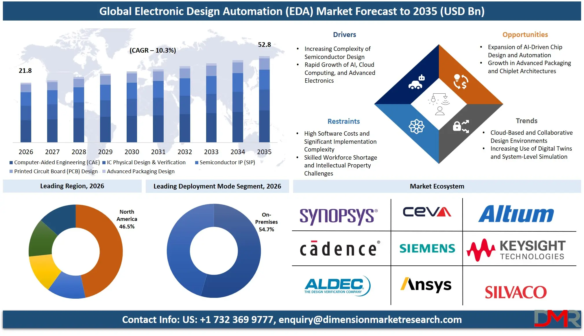
The Electronic Design Automation (EDA) Market size is expected to be USD 21.8 billion in 2026 and increase at a compound annual growth rate of 10.3% to USD 52.8 billion in 2035 due to increasing design complexity in semiconductors.
ℹ
To learn more about this report –
Download Your Free Sample Report Here
The EDA market is an oligopoly that is technology-intensive, and the competitive pressure in this market stems from innovation, product integrations, and ecosystems. Firms in the EDA industry place great importance on researching and developing in order to increase the quality of simulations, enhance artificial intelligence design abilities, and offer more cloud-based solutions. Cooperation with chipmakers, foundry facilities, and cloud computing providers is essential for firms to position themselves competitively in this industry. Barriers to entry in this industry are quite high due to large demands for intellectual property, engineering complexity, and lengthy development periods. The competitive advantage in this industry stems from interoperable tools, effective design, and compatibility with new chip architectures like chiplets and 3D ICs.
The US Electronic Design Automation (EDA) Market
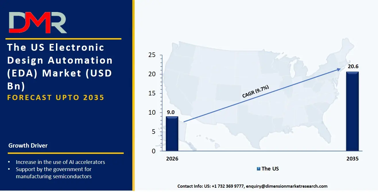
The US Electronic Design Automation (EDA) Market size is estimated to be USD 9.0 billion in 2026 and is expected to increase at a CAGR of 9.7% over the forecast period.
ℹ
To learn more about this report –
Download Your Free Sample Report Here
Being technologically advanced and having the highest number of semiconductor manufacturers and world-class technology companies makes the United States the biggest and leading market for Electronic Design Automation tools. The increase in the use of AI accelerators, data center processors, defense electronics, and advanced automotive semiconductors has further increased the demand for advanced EDA software tools. The support by the government for manufacturing semiconductors within the country and collaborations between semiconductor chip developers and cloud services have improved the position of the country in terms of its market. Innovation in designing of electronic systems has also contributed to the adoption of EDA tools in different fields.
Europe Electronic Design Automation (EDA) Market
The Europe Electronic Design Automation (EDA) Market size is estimated to be USD 4.1 billion in 2026 and is expected to increase at a CAGR of 9.6% over the forecast period.
Europe emerges as a key market of Electronic Design Automation because of the presence of powerful automotive electronics production, industrial automation processes, aerospace innovations, and sustainability-oriented semiconductor programs. The regional policy promoting semiconductor autonomy and digitalization is spurring investment in sophisticated chip design tools. Growing popularity of electric vehicles, Industry 4.0 trends, and semiconductor security chains is increasing the need for Electronic Design Automation solutions. Joint research between universities, semiconductor producers, and technology companies also plays an important role in innovations, along with the development of sophisticated packaging and system design tools.
Japan Electronic Design Automation (EDA) Market
The market size of Japan Electronic Design Automation (EDA) will be USD 1.1 billion in 2026 and at a CAGR of 10.1% in the forecast period.
Japan is continuously improving its position in the Electronic Design Automation market thanks to its advancements in technology regarding the production of semiconductors, precision manufacturing, automotive electronics, robotics, and industrial automation. Growing investment in semiconductor manufacturing, AI chips, and other electronic products results in increasing the need for efficient design automation tools. The government support for the semiconductor revamping, strategic cooperation with international chip producers, as well as research on innovative packaging technologies, all result in market growth.
Key Takeaways
- Market Size & Forecast: The Electronic Design Automation (EDA) Market size is projected to reach USD 21.8 billion in 2026 and is anticipated to have a value of USD 52.8 billion in 2035.
- Growth Rate & Outlook: The Electronic Design Automation (EDA) Market size is set to grow at a compound annual growth rate of 10.3% during the forecast period of 2026 to 2035.
- Primary Growth Drivers: Some of the major growth drivers in the market are Increasing Design Complexity in Semiconductors and more.
- Key Market Trends: Some of the major trends in the market are Cloud-based and Collaborative Design Environment more.
- By Product Type: CAE segment is anticipated to get the majority share of the Electronic Design Automation (EDA) Market in 2026.
- By End User Type: Fabless Semiconductor Companies are expected to get the largest revenue share in 2026 in the Electronic Design Automation (EDA) Market.
- By Deployment Type: On-Premise is expected to get the largest revenue share in 2026 in the Electronic Design Automation (EDA) Market.
- Regional Leadership: North America is set to lead the Electronic Design Automation (EDA) Market with an estimated 46.5% share in 2026.
What is the Electronic Design Automation (EDA)?
Electronic Design Automation (EDA) is an array of software-based and hardware-based methods utilized in designing, verifying, simulating, testing, and manufacturing semiconductor integrated circuits (ICs), printed circuit boards (PCBs), and electronic systems. The tools include such advanced technologies as logic synthesis, functional verification, timing analysis, physical design, signal integrity analysis, thermal simulation, semiconductor IP, and advanced packaging design. EDA is critically important because it allows engineers to handle chip complexity, decrease design cycles, increase manufacturing efficiency, and innovate rapidly in such areas as consumer electronics, automotive industry, aerospace industry, telecom industry, industrial automation, and health care. The emerging developments like AI-assisted chip design, cloud-native EDA solutions, chiplets, and heterogeneous integration are revolutionizing the area of EDA.
Use Cases
- Designing Semiconductor Chips: The use of EDA tools allows designers to design very intricate integrated circuits that are employed in processing devices, storage devices, accelerators, and communication chips. Automation greatly decreases the chances of making errors in the designing process, saves time, and helps improve manufacturing processes.
- Development of Automotive Electronics: EDA technologies are used by automakers to design electronic control units, processors for self-driving cars, battery systems, and car communication systems.
- Development of Consumer Electronics: EDA tools are very useful when it comes to designing consumer electronic devices such as phones, wearables, games consoles, and smart home devices because they help designers to optimize ICs, design PCBs, verify the designs, and analyze thermal performance of these devices.
- Applications of EDA Tools in Aerospace and Defense Industries: Designers use EDA technologies to design extremely reliable electronic devices that are used in satellites, radar systems, communication devices, avionics, and defense computers.
How AI Is Transforming the Electronic Design Automation (EDA) Market
The field of Electronic Design Automation is being revolutionized through artificial intelligence, where design efficiency, automation accuracy, and optimization are greatly improved. AI algorithms can be used for chip floorplanning, placement, routing, and optimization of timing, making the process easier and fast. Prediction of bottlenecks in designs, improvement of power efficiency, and performance tradeoffs can be done using machine learning models, leading to quicker decision-making.
AI is being used in the verification process to detect errors and inconsistencies in designs, hence improving the reliability of chips. Moreover, the use of generative AI is increasing in proposing optimized circuit designs to reduce the complexity of the process. These improvements have allowed semiconductor companies to become more productive and save costs and time.
Market Dynamic
Driving Factors in the Electronic Design Automation (EDA) Market
Increasing Design Complexity in Semiconductors
Today's semiconductor components contain billions of transistors on a single chip. This is why the traditional methods of designing such chips have become unfeasible. The increasing use of artificial intelligence processors, autonomous driving systems, high-performance computing, 5G technologies, and edge computing has led to greater design complexity. Using Electronic Design Automation software allows the designers to automate the tasks of verification, timing analysis, simulations, physical design, and optimization. Such solutions not only decrease design risks but also enhance its quality.
Restraints in the Electronic Design Automation (EDA) Market
High Cost of Software Licenses and Complex Implementation Process
High costs of software licenses and investment in powerful computing systems, engineering staff, and training of employees are associated with the usage of Electronic Design Automation systems. Small and mid-cap semiconductor firms may lack sufficient funding to use fully-fledged EDA tools due to the presence of financial restrictions. Furthermore, integration of a number of design programs into engineering processes is a complicated process which may take much time.
Opportunities in the Electronic Design Automation (EDA) Market
Increase in AI-Powered Chip Design and Automation
The adoption of artificial intelligence in the semiconductor design process is one of the biggest growth drivers for the Electronic Design Automation industry. The use of such tools in layout optimization, circuit verification, design rule checks, and power, performance, area optimizations greatly decreases the design cycle time and increases efficiency, allowing designers to explore bigger design spaces. With the increase in chip complexity, the need for AI-powered EDA software is predicted to become crucial, thus providing good opportunities for companies which offer such solutions.
Trends in the Electronic Design Automation (EDA) Market
Cloud-based and Collaborative Design Environment
The usage of cloud technology in the semiconductor design industry has revolutionized the EDA sector through scalability of computing, remote collaboration, and rapid simulation processes. Cloud-based EDA tools allow multiple teams of engineers to collaboratively work on designs from a cloud computing environment without the need for significant infrastructure. Such changes have made the process more efficient, lowered capital investment requirements, and allowed startups and smaller companies to gain access to design features available only to major semiconductor companies.
Research Scope and Analysis
The Electronic Design Automation (EDA) market research gauges the performance of the industry by assessing product types, deployment modes, user verticals, and geographical segments. Technological developments, new demands in semiconductor design, market drivers, limitations, opportunities, competition, and innovation trends have been thoroughly investigated. In addition, the study considers adoption trends, investment trends, and future potential.
ℹ
To learn more about this report –
Download Your Free Sample Report Here
By Product Analysis
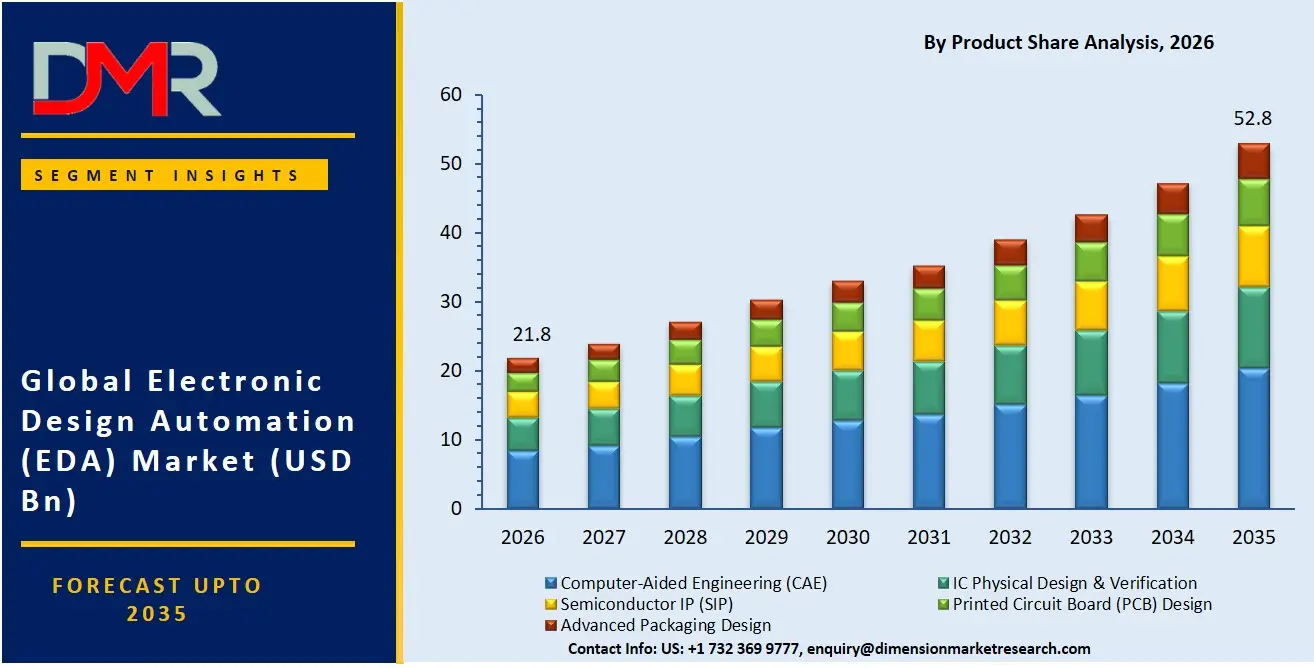
In the Electronic Design Automation market, segments include CAE, IC physical design & verification, SIP, and PCB design. Of all these segments, the IC physical design & verification segment will capture the maximum share of the market by 2026 at 38.4%. This is mainly owing to the increasing complexity of chips and requirement for validation of highly performing processors, AI chips, and semiconductor automotive applications. This segment profits from the increasing demand for layout design, timing closure, and manufacturability.
ℹ
To learn more about this report –
Download Your Free Sample Report Here
The SIP segment represents the fastest-growing segment as there is a rapid increase in the adoption of reusable components of chip design such as processors IP, interface IP, and memory IP. This reduces development costs and time significantly.
By Deployment Mode Analysis
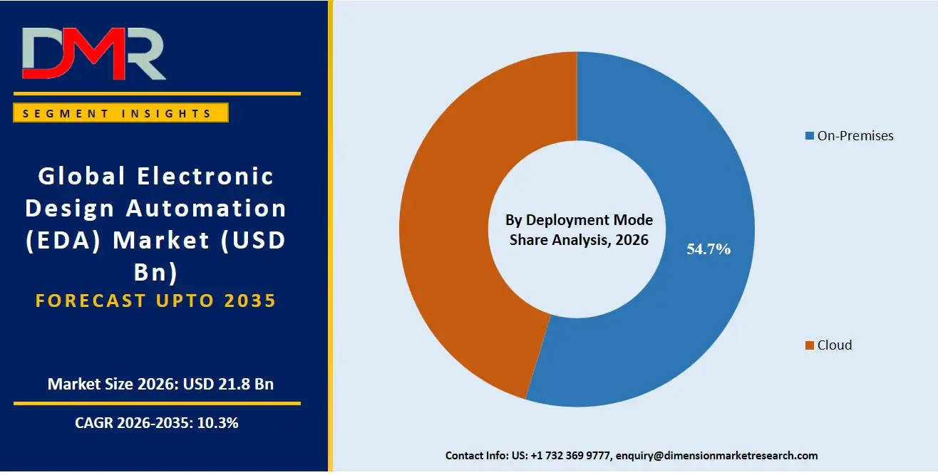
On the basis of Deployment Mode, the market has been categorized into On-Premises and Cloud-Based segments. The former will lead the market during forecast period with market share of 54.7% in 2026 owing to security issues, intellectual property issues, and enterprise infrastructure of semiconductor giants. The On-Premise system provides more control on sensitive information related to chip design and is popularly deployed by industries like Aerospace & Defense.
But Cloud-based EDA is witnessing the fastest growth rate owing to scalability of computing power, ease of collaboration, and cost-effectiveness.
By End User Analysis
The global market is divided into Fabless Semiconductor Companies, Integrated Device Manufacturers (IDMs), Foundries, Electronic System & OEM Companies, Automotive Electronics Companies, Aerospace & Defense Companies, Consumer Electronics Companies, Telecommunication Companies, and Industrial Electronics Companies. Out of all these segments, Fabless Semiconductor Companies hold a dominant position in the market with a projected share of 41.2% in 2026 because of the high use of EDA software in the design of chips without possessing any manufacturing facilities.
The automotive electronics companies account for the highest growth rate in the end-user segment as they have a growing need for electric cars, autonomous vehicles, and driver-assisted technologies.
The Electronic Design Automation (EDA) Market Report is segmented on the basis of the following:
By Product
- Computer-Aided Engineering (CAE)
- Functional Verification
- Logic Simulation
- Physical & Thermal Analysis
- IC Physical Design & Verification
- Semiconductor IP (SIP)
- Processor IP
- Interface IP
- Memory IP
- Analog & Mixed-Signal IP
- Printed Circuit Board (PCB) Design
- Advanced Packaging Design
By Deployment Mode
By End User
- Fabless Semiconductor Companies
- Integrated Device Manufacturers (IDMs)
- Foundries
- Electronic System & OEM Companies
- Automotive Electronics Companies
- Aerospace & Defense Organizations
- Consumer Electronics Manufacturers
- Telecommunications Companies
- Industrial Electronics Companies
Regional Analysis
Leading Region in the Electronic Design Automation (EDA) Market
ℹ
To learn more about this report –
Download Your Free Sample Report Here
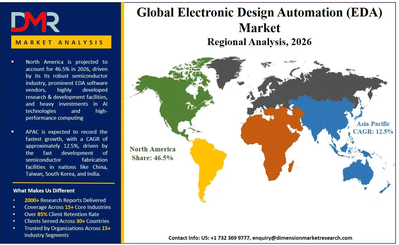
The North American region is the leader in the Electronic Design Automation market with an expected market share of 46.5% in 2026 owing to its robust semiconductor industry, prominent EDA software vendors, highly developed research & development facilities, and heavy investments in AI technologies and high-performance computing. The contribution of fabless semiconductor companies, hyperscale cloud companies, and defense electronics companies is a vital factor that drives the demand for advanced design software solutions. Government incentives to promote the manufacture of semiconductor chips domestically through the CHIPS Act bolster market growth.
Fastest Growing Region in the Electronic Design Automation (EDA) Market
Asia-Pacific has emerged as the fastest growing region in the Electronic Design Automation (EDA) market owing to the fast development of semiconductor fabrication facilities in nations like China, Taiwan, South Korea, and India. The increasing spending on chip fabrication facilities, consumer electronics manufacturing, and automotive electronics is driving the need for EDA products in the region. Other growth drivers include government support towards semiconductor independence, increasing use of AI technologies, and presence of electronics supply chain across the globe. The region offers the advantage of having a vast engineering workforce along with investments in R&D, thus becoming an important growth engine for the global EDA market.
By Region
North America
Europe
- Germany
- The U.K.
- France
- Italy
- Russia
- Spain
- Benelux
- Nordic
- Rest of Europe
Asia-Pacific
- China
- Japan
- South Korea
- India
- ANZ
- ASEAN
- Rest of Asia-Pacific
Latin America
- Brazil
- Mexico
- Argentina
- Colombia
- Rest of Latin America
Middle East & Africa
- Saudi Arabia
- UAE
- South Africa
- Israel
- Egypt
- Rest of MEA
Competitive Landscape
The EDA market is an oligopoly that is technology-intensive, and the competitive pressure in this market stems from innovation, product integrations, and ecosystems. Firms in the EDA industry place great importance on researching and developing in order to increase the quality of simulations, enhance artificial intelligence design abilities, and offer more cloud-based solutions. Cooperation with chipmakers, foundry facilities, and cloud computing providers is essential for firms to position themselves competitively in this industry. Barriers to entry in this industry are quite high due to large demands for intellectual property, engineering complexity, and lengthy development periods. The competitive advantage in this industry stems from interoperable tools, effective design, and compatibility with new chip architectures like chiplets and 3D ICs.
Some of the prominent players in the global Electronic Design Automation (EDA) are:
- Synopsys
- Cadence Design Systems
- Siemens EDA
- Ansys
- Keysight Technologies
- Silvaco
- Altium
- Zuken
- Primarius Technologies
- Empyrean Technology
- Xpeedic Technology
- Aldec
- Arteris
- CEVA
- Rambus
- Imagination Technologies
- Alphawave IP Group
- Agnisys
- Verific Design Automation
- Cliosoft
- Other Key Players
Recent Developments
- In May 2026, Through the "Zuken Valeo InnoLab," Valeo and Zuken are working towards establishing a strategic partnership where both firms will collaborate to create an AI-enabled electronic design system. The partnership involves integrating the artificial intelligence technologies used by Zuken in EDA (electronic design automation) with those of Valeo, who uses AI agents, to create an interactive engineer-AI collaboration.
- In April 2026, The 2026 edition of Mouser Electronics' technology series called Empowering Innovation Together (EIT) titled "Engineering AI for Daily Life" was introduced to emphasize the increasing use of artificial intelligence in everyday products and services. The program discusses how AI is being utilized in consumer electronics, connected technologies, healthcare wearable, and digital solutions and stresses the importance of engineers in building effective, easy-to-use, and trustworthy AI solutions.
- In April 2026, Synopsys launched an enhanced version of AI-based electronic design automation technology, which is designed for the cutting-edge processes and packaging technologies of TSMC that include 3 nm, 2 nm, A16, and A14 process nodes. This enhancement will include the application of AI-based digital, analog, verification, and 3D multi-die flows and proven silicon IPs in order to speed up the design of semiconductors.
Report Details
| Report Characteristics |
| Market Size (2026) |
USD 21.8 Bn |
| Forecast Value (2035) |
USD 52.8 Bn |
| CAGR (2026–2035) |
10.3% |
| Historical Period |
2021 – 2025 |
| Forecast Period |
2027 – 2035 |
| Base Year |
2025 |
| Estimate Year |
2026 |
| Segments Covered |
By Product, By Deployment Mode, By End User |
| Regional Coverage |
North America – The US and Canada; Europe – Germany, The UK, France, Russia, Spain, Italy, Benelux, Nordic, & Rest of Europe; Asia-Pacific – China, Japan, South Korea, India, ANZ, ASEAN, Rest of APAC; Latin America – Brazil, Mexico, Argentina, Colombia, Rest of Latin America; Middle East & Africa – Saudi Arabia, UAE, South Africa, Turkey, Egypt, Israel, & Rest of MEA |
Frequently Asked Questions
How big is the Electronic Design Automation (EDA) Market?
▾ The Electronic Design Automation (EDA) Market size is expected to reach USD 21.8 billion by 2026 and is projected to reach USD 52.8 billion by the end of 2035.
What is the CAGR of the Electronic Design Automation (EDA) Market from 2026 to 2035?
▾ The market is growing at a CAGR of 10.3 percent over the forecasted period.
What factors are driving the growth of the Electronic Design Automation (EDA) Market?
▾ Increasing Design Complexity in Semiconductors, and more are the factors driving the growth of the Electronic Design Automation (EDA) Market.
What are the major trends in the Electronic Design Automation (EDA) Market?
▾ Cloud-based and Collaborative Design Environment, and more are some of the major trends in the market.
Who are the key players in the Electronic Design Automation (EDA) Market?
▾ Some of the key players in the Electronic Design Automation (EDA) Market include Ceva, Ansys, Siemens and more.
How is the Electronic Design Automation (EDA) Market segmented?
▾ The Electronic Design Automation (EDA) Market is segmented by product, deployment mode, end user.
Which region held the largest share of the Electronic Design Automation (EDA) Market in 2026?
▾ North America is set to lead the Electronic Design Automation (EDA) Market with an estimated 46.5% share in 2026.
Which region is expected to grow the fastest in the Electronic Design Automation (EDA) Market?
▾ Asia Pacific is the fastest-growing region in the Electronic Design Automation (EDA) Market during the forecast period.