Market Overview
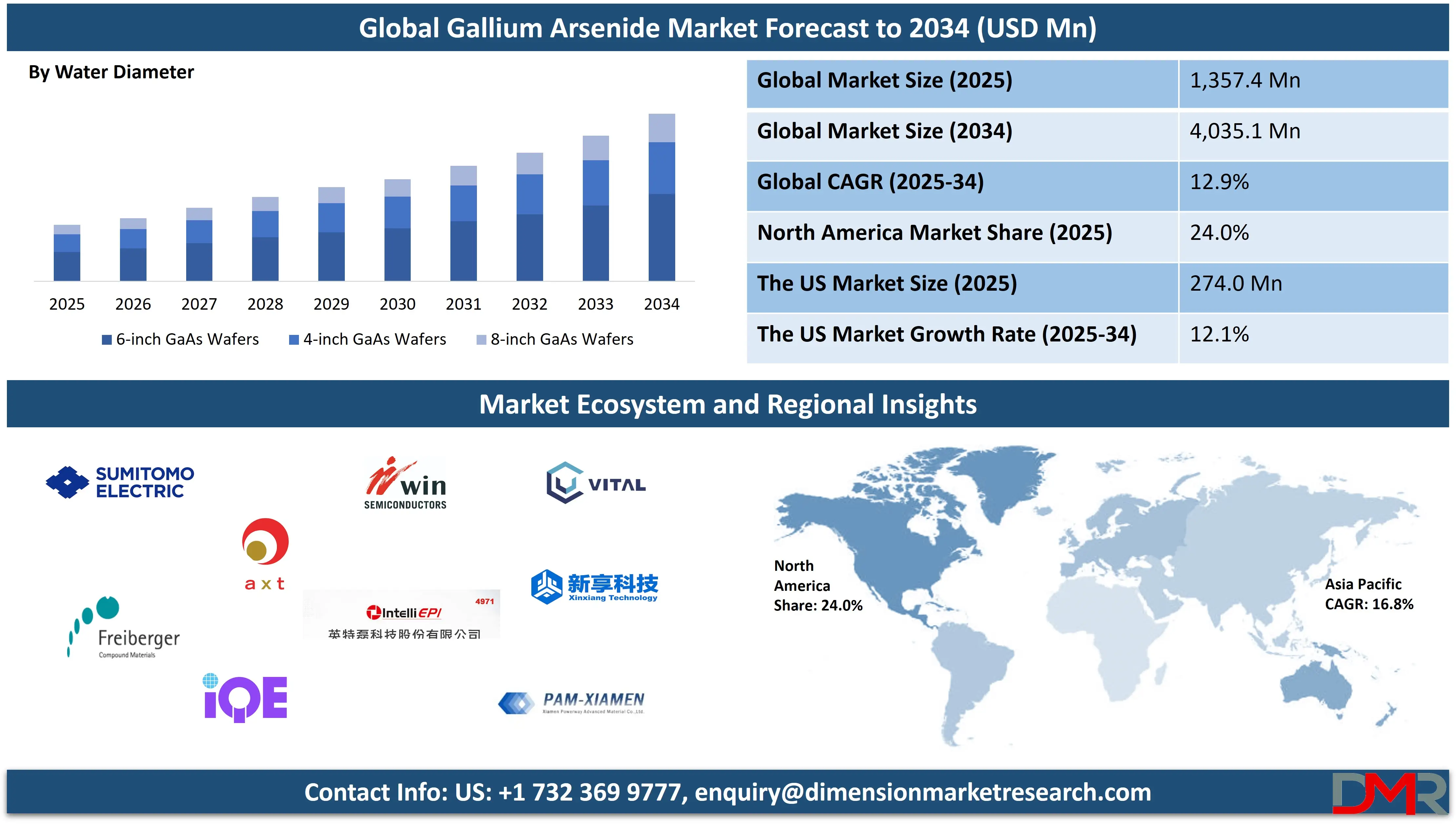
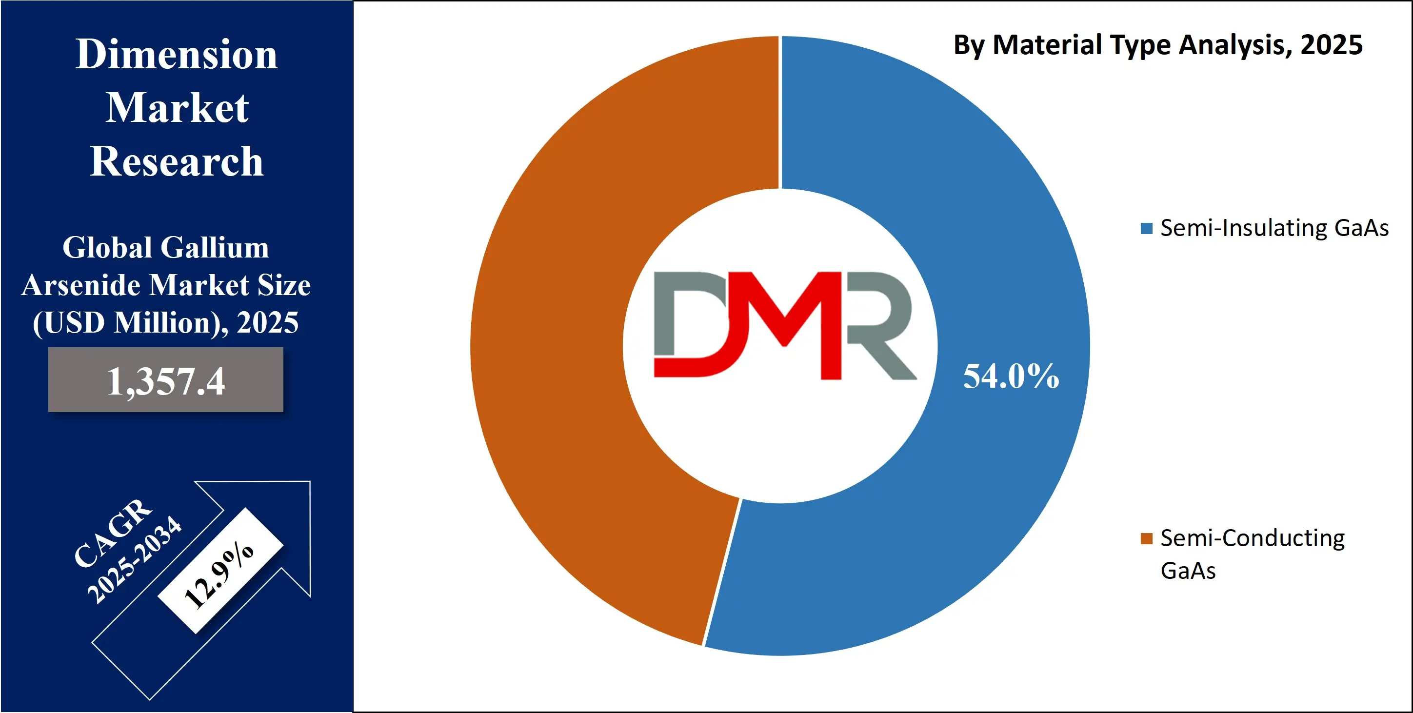
The global Gallium Arsenide market was valued at USD 1,357.4 million in 2025 and is expected to reach USD 4,035.1 million by 2034, expanding at a CAGR of 12.9%, driven by rising demand for compound semiconductors, RF devices, optoelectronics, 5G infrastructure, high speed electronics and advanced wireless communication technologies.
ℹ
To learn more about this report –
Download Your Free Sample Report Here
Gallium Arsenide (GaAs) is a compound semiconductor material formed by combining gallium and arsenic in a crystalline lattice that delivers superior electronic and optical performance compared to traditional silicon. It offers high electron mobility, wide bandgap characteristics and strong resistance to heat and radiation, making it ideal for high frequency, high power and optoelectronic applications. GaAs enables faster signal processing, lower power consumption and higher efficiency in devices such as microwave integrated circuits, laser diodes, light emitting diodes and photovoltaic cells, which is why it is widely used in advanced communication, sensing and energy technologies.
The global Gallium Arsenide market represents the worldwide ecosystem of companies involved in the production, processing and commercialization of GaAs substrates, wafers, epitaxial layers and semiconductor devices used across multiple industries. This market is driven by the rising deployment of 5G networks, expanding satellite communications, growing demand for radio frequency components in smartphones and increasing adoption of compound semiconductors in defense, aerospace and high speed data transmission. Manufacturers focus on improving wafer quality, scaling wafer sizes and enhancing crystal growth technologies to meet the evolving performance requirements of modern electronics.
ℹ
To learn more about this report –
Download Your Free Sample Report Here
At a broader level, the global GaAs market also includes a wide range of applications such as optoelectronics, solar energy systems, automotive radar, lidar and advanced sensors, all of which benefit from the material’s high efficiency and signal integrity. As digital infrastructure, autonomous systems and optical communication networks continue to expand, GaAs based devices are gaining importance for enabling faster connectivity, greater energy efficiency and improved reliability. This makes the global Gallium Arsenide market a critical part of the next generation semiconductor landscape supporting wireless, photonic and power electronic innovation.
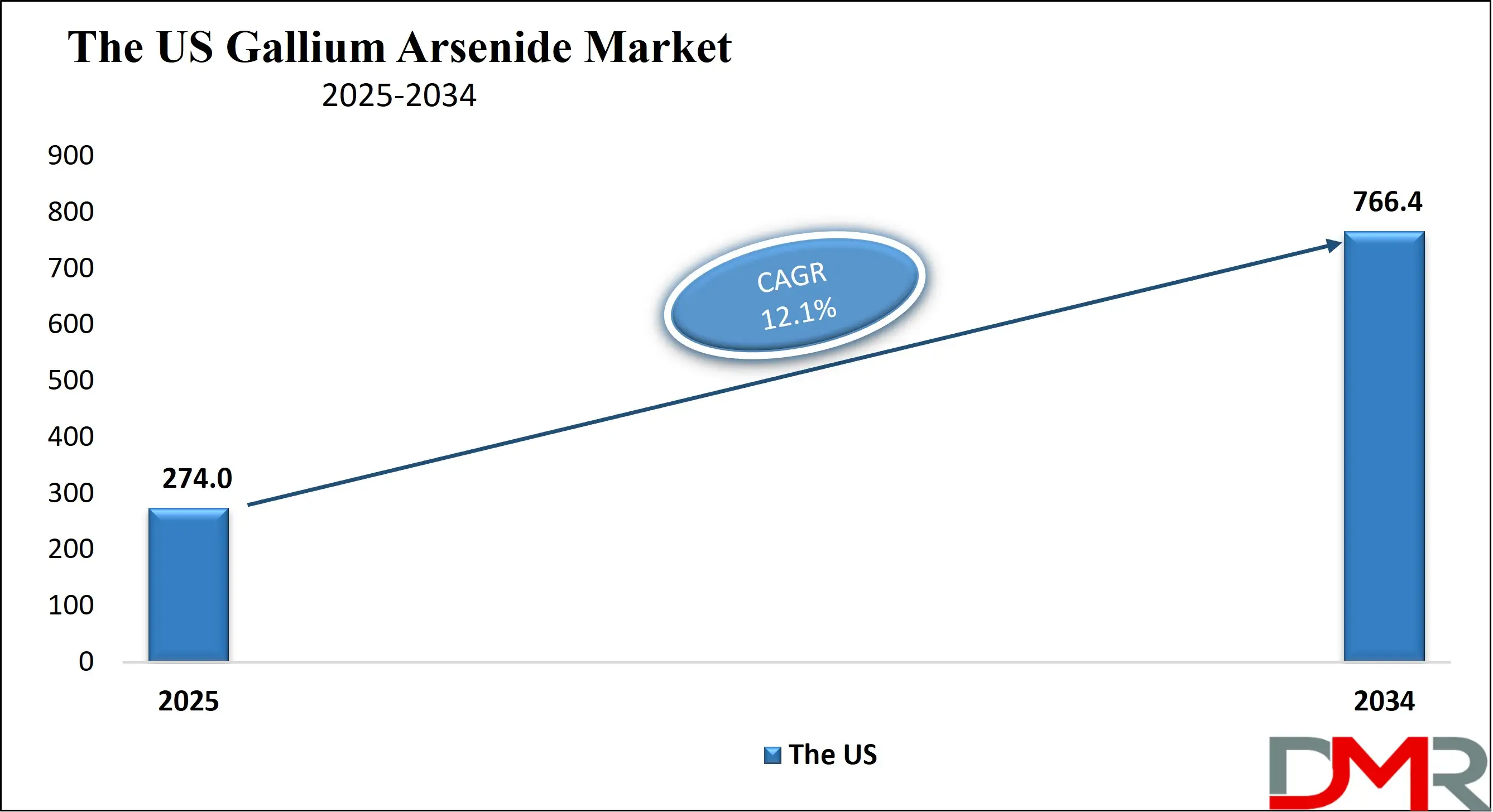
The US Gallium Arsenide Market
The U.S. Gallium Arsenide Market size was valued at USD 274.0 million in 2025. It is further expected to witness subsequent growth in the upcoming period, holding USD 766.4 million in 2034 at a CAGR of 12.1%.
ℹ
To learn more about this report –
Download Your Free Sample Report Here
The US Gallium Arsenide market is driven by the country’s strong presence in advanced semiconductor manufacturing, defense electronics and next generation wireless infrastructure. High demand for RF power amplifiers, microwave integrated circuits and optoelectronic components from 5G base stations, satellite communications and data centers continues to accelerate GaAs adoption. The United States also benefits from a mature ecosystem of material suppliers, wafer fabricators and device manufacturers that support innovation in high speed, high frequency and high reliability semiconductor applications across aerospace, telecommunications and industrial sectors.
Growth in the US GaAs market is further supported by rising investments in defense modernization, space exploration and autonomous technologies, where compound semiconductors outperform silicon in extreme environments. Applications such as radar systems, lidar sensors, secure communications and infrared imaging rely heavily on GaAs based components for superior signal integrity and power efficiency. In parallel, the expansion of electric vehicles, advanced driver assistance systems and optical networking is increasing the need for high performance optoelectronics and RF chips, strengthening long term demand for Gallium Arsenide across the United States.
Europe Gallium Arsenide Market
The Europe Gallium Arsenide market was valued at USD 176.5 million in 2025, reflecting steady demand across key industrial and technological sectors. The market is primarily driven by the adoption of high frequency and high power electronic components in telecommunications, defense, aerospace, and automotive applications. European manufacturers and technology firms are investing in GaAs wafers, RF modules, and optoelectronic devices to support 5G infrastructure, satellite communication systems, and advanced radar applications. The availability of skilled labor and established semiconductor fabrication facilities also supports consistent growth in the region.
The market in Europe is expected to grow at a CAGR of 10.9% over the forecast period, indicating moderate but sustained expansion. This growth is fueled by increasing investments in advanced communication networks, defense modernization programs, and the rising adoption of GaAs-based devices in industrial automation and consumer electronics. Additionally, initiatives to improve energy efficiency and reduce device size in optoelectronic and RF applications are encouraging further use of GaAs technology. As European companies continue to focus on innovation and high-performance components, the region is likely to maintain a strong position in the global GaAs market.
Japan Gallium Arsenide Market
The Japan Gallium Arsenide market was valued at USD 67.9 million in 2025, driven by strong adoption of advanced semiconductor technologies in telecommunications, consumer electronics, and industrial automation. Japanese companies are investing in GaAs wafers, RF components, and optoelectronic devices to support 5G networks, high-speed data communication, and satellite systems. The country’s established electronics and semiconductor manufacturing ecosystem, along with skilled engineering capabilities, allows for efficient production of high-quality GaAs-based devices, contributing to the steady demand in both domestic and export markets.
The market in Japan is projected to grow at a CAGR of 12.8%, closely aligned with the global growth trend, reflecting increasing demand for high frequency, low power, and high performance electronic components. Rising investments in automotive radar, lidar sensors, and defense electronics further strengthen market prospects, while continuous innovation in device design and wafer fabrication ensures Japan remains competitive in the global GaAs landscape. Expansion in optoelectronics and photonics applications also supports long-term growth opportunities in the region.
Global Gallium Arsenide Market: Key Takeaways
- Strong Demand for Compound Semiconductors: High frequency, high power, and optoelectronic applications in 5G, aerospace, and defense are driving GaAs adoption globally.
- Asia Pacific Leads the Market: China, Japan, South Korea, and Taiwan dominate production and device fabrication, accounting for over half of global revenue.
- Advancements in Wafer and Crystal Growth: LEC and VGF technologies, along with 6-inch and 8-inch wafers, improve yield, uniformity, and device performance.
- Wide-Ranging Applications: GaAs is critical in RF/microwave devices, optoelectronics, photonics, autonomous systems, and edge computing.
- Opportunities amid Challenges: High costs and complex manufacturing are offset by growth in EVs, defense, space, and AI-driven semiconductor applications.
Global Gallium Arsenide Market: Use Cases
- 5G and Wireless Communication Infrastructure: Gallium Arsenide is widely used in 5G base stations and wireless networks for RF power amplifiers and microwave circuits. Its high frequency performance and low signal loss support faster data transmission, stable connectivity and efficient network operations in modern telecom infrastructure.
- Smartphones and Consumer Electronics: GaAs enables high performance RF front end modules in smartphones and connected devices. It improves signal quality, data speeds and power efficiency, making it essential for 5G enabled mobile phones and compact wireless electronics.
- Aerospace and Defense Systems: GaAs is used in radar, satellite communication and electronic warfare systems due to its reliability under extreme conditions. Its high power and high frequency capabilities support secure communication, tracking and surveillance technologies.
- Optoelectronics and Solar Energy: Gallium Arsenide supports LEDs, laser diodes and high efficiency solar cells. These applications benefit from its superior light conversion, energy efficiency and durability, making it valuable for displays, optical networks and space based solar power.
Impact of Artificial Intelligence on the global Gallium Arsenide market
Artificial Intelligence is increasingly shaping the global Gallium Arsenide market by driving demand for high performance semiconductors capable of supporting complex data processing and high speed connectivity. AI applications in data centers, edge computing and neural network accelerators require components that deliver low latency, high frequency and efficient power handling, areas where GaAs based RF and microwave devices offer advantages over traditional silicon. As AI workloads grow, telecommunication networks need greater bandwidth and faster signal processing, boosting adoption of GaAs in 5G and future 6G infrastructure to support machine-to-machine communication and real-time analytics.
In addition, AI-enabled automated design and manufacturing tools are accelerating GaAs device development through improved yield optimization, predictive maintenance and precise process control. These tools help reduce production costs, increase wafer throughput and enhance material uniformity, making GaAs technology more competitive. AI algorithms also enable smarter resource allocation and real-time quality monitoring in fabrication facilities, strengthening supply chain efficiency. As AI integration expands across automotive, aerospace and industrial IoT, the need for high frequency, high reliability GaAs components is expected to rise, further expanding the global market for compound semiconductors.
Global Gallium Arsenide Market: Stats & Facts
-
U.S. Geological Survey (USGS) / U.S. Government Sources
- In the United States, about 79 % of gallium consumed is in the form of GaAs, GaN, and GaP wafers used in semiconductors and optoelectronics.
- Domestic primary (low‑purity) gallium has not been produced in the U.S. since 1987 and demand is met entirely by imports.
- Gallium consumed in epitaxial layering for wafers (GaAs epiwafers) accounts for most remaining consumption after integrated circuits.
- Analog and digital integrated circuits accounted for 74 % of gallium consumption in the U.S. in recent years.
- Optoelectronic devices such as lasers, LEDs, photodetectors and solar cells accounted for 20 % of gallium consumption.
- In 2024, the value of imported gallium arsenide wafer imports into the U.S. was approximately USD 140 million, up 24 % from 2023.
- Gallium metal imports into the U.S. were valued at approximately USD 4 million in 2024.
- About 83 % of the gallium consumed in the U.S. in 2024 was used in GaAs, GaN, and GaP wafers.
- USGS Historical Import Data (2023)
- In 2023 the value of imported gallium metal into the U.S. was about USD 3 million, showing significant volatility year‑over‑year.
- In 2023 GaAs wafer imports into the U.S. were valued at about USD 110 million, down roughly 50 % from 2022.
- In 2023 approximately 79 % of gallium consumption in the U.S. continued to be in GaAs, GaN and GaP wafers.
- Gallium Supply Chain Context (Global, US Government Referenced)
- As of 2024, China produced about 98 % of the world’s low‑purity gallium, a key input for GaAs.
- GaAs and GaN together comprise the vast majority of commercial gallium usage in U.S. semiconductors.
- In the early 2000s, worldwide GaAs made up approximately 95 % of annual gallium consumption, reflecting its enduring structural importance to semiconductors.
- Gallium arsenide’s high‑efficiency properties historically made it critical in RF, wireless and optoelectronics applications.
Global Gallium Arsenide Market: Market Dynamics
Global Gallium Arsenide Market: Driving Factors
Rising deployment of 5G and advanced wireless networks
The rapid rollout of 5G infrastructure and high speed wireless communication is significantly driving the Gallium Arsenide market. GaAs based RF power amplifiers, microwave integrated circuits and radio frequency components provide superior signal strength, low noise and high frequency performance compared to silicon. As telecom operators expand base stations, small cells and satellite networks, demand for compound semiconductors such as GaAs continues to rise to support faster data transfer, improved network efficiency and reliable connectivity.
Growth in optoelectronics and high speed electronics
Increasing use of laser diodes, LEDs, optical sensors and high speed communication devices is accelerating GaAs adoption. Industries such as data centers, autonomous vehicles and industrial automation rely on GaAs based optoelectronic devices for precise signal transmission, energy efficiency and high reliability. This broadening application base strengthens long term market growth.
Global Gallium Arsenide Market: Restraints
High production and material costs
Gallium Arsenide wafers and epitaxial layers are more expensive to produce than silicon due to complex crystal growth processes and limited raw material availability. These higher costs can restrict large scale adoption, especially in price sensitive consumer electronics and mass production semiconductor applications.
Manufacturing complexity and lower yield rates
The fabrication of GaAs devices requires specialized equipment and controlled environments. Lower wafer yields, sensitivity to defects and limited foundry capacity compared to silicon can slow down production scalability and impact overall market penetration.
Global Gallium Arsenide Market: Opportunities
Expansion of electric vehicles and advanced driver systems
The increasing use of automotive radar, lidar and high frequency sensing in electric and autonomous vehicles creates strong growth opportunities for GaAs. These systems rely on compound semiconductors for accurate detection, low power consumption and reliable performance under harsh conditions.
Rising investments in space and defense electronics
Growing spending on satellite communications, space exploration and defense modernization opens new opportunities for GaAs manufacturers. High efficiency solar cells, secure communication systems and advanced radar platforms all benefit from the superior electronic properties of Gallium Arsenide.
Global Gallium Arsenide Market: Trends
Shift toward larger wafer sizes and improved epitaxy
Manufacturers are moving toward 6 inch and 8 inch GaAs wafers along with advanced epitaxial growth technologies to improve device performance and production efficiency. This trend supports higher output, better uniformity and lower cost per device.
Integration of GaAs in photonic and AI driven systems
GaAs is increasingly being used in photonics, optical interconnects and AI driven communication hardware. The demand for faster data processing, edge computing and machine learning applications is pushing the adoption of high speed, low latency GaAs based components in next generation electronic systems.
Global Gallium Arsenide Market: Research Scope and Analysis
By Material Type Analysis
Semi insulating Gallium Arsenide is expected to dominate the material type segment with a 54.0% share in 2025 because it is the preferred substrate for high frequency and high power electronic devices used in wireless communication, satellite systems and radar applications. Its extremely high resistivity allows excellent electrical isolation between components, which reduces signal leakage, minimizes interference and improves device reliability. This makes it ideal for RF integrated circuits, microwave devices and power amplifiers used in 5G infrastructure, aerospace electronics and advanced networking equipment, where signal purity and stability are critical.
ℹ
To learn more about this report –
Download Your Free Sample Report Here
Semi conducting Gallium Arsenide also plays a vital role in this market segment, particularly in optoelectronic and active electronic applications. Doped GaAs materials are used to manufacture laser diodes, light emitting diodes, photodetectors and high speed transistors that require controlled electrical conductivity. These materials support efficient charge carrier movement, high switching speeds and strong light emission properties, which are essential for optical communication, data centers, sensing technologies and solar cells. Together, semi insulating and semi conducting GaAs enable a wide range of high performance compound semiconductor applications across global electronics and photonics industries.
By Crystal Growth Technology Analysis
Liquid Encapsulated Czochralski is expected to dominate the crystal growth technology segment with a 56.0% share in 2025 because it has been the most widely adopted and commercially proven method for producing high quality Gallium Arsenide wafers. LEC technology allows stable crystal growth with good diameter control and high throughput, making it suitable for mass production of GaAs substrates used in RF devices, microwave circuits and optoelectronic components. Its long established manufacturing base, compatibility with existing fabrication lines and consistent wafer availability continue to support its strong position across telecom, defense and consumer electronics applications.
Vertical Gradient Freeze also plays an important role in this market segment, particularly for applications that require higher purity, lower defect density and improved crystal uniformity. VGF grown GaAs wafers offer better control over thermal gradients during solidification, which reduces dislocations and improves electrical performance. This makes VGF technology increasingly attractive for advanced optoelectronics, high speed devices and next generation RF components. As demand rises for higher performance and larger diameter wafers, VGF adoption is gradually increasing alongside traditional LEC methods.
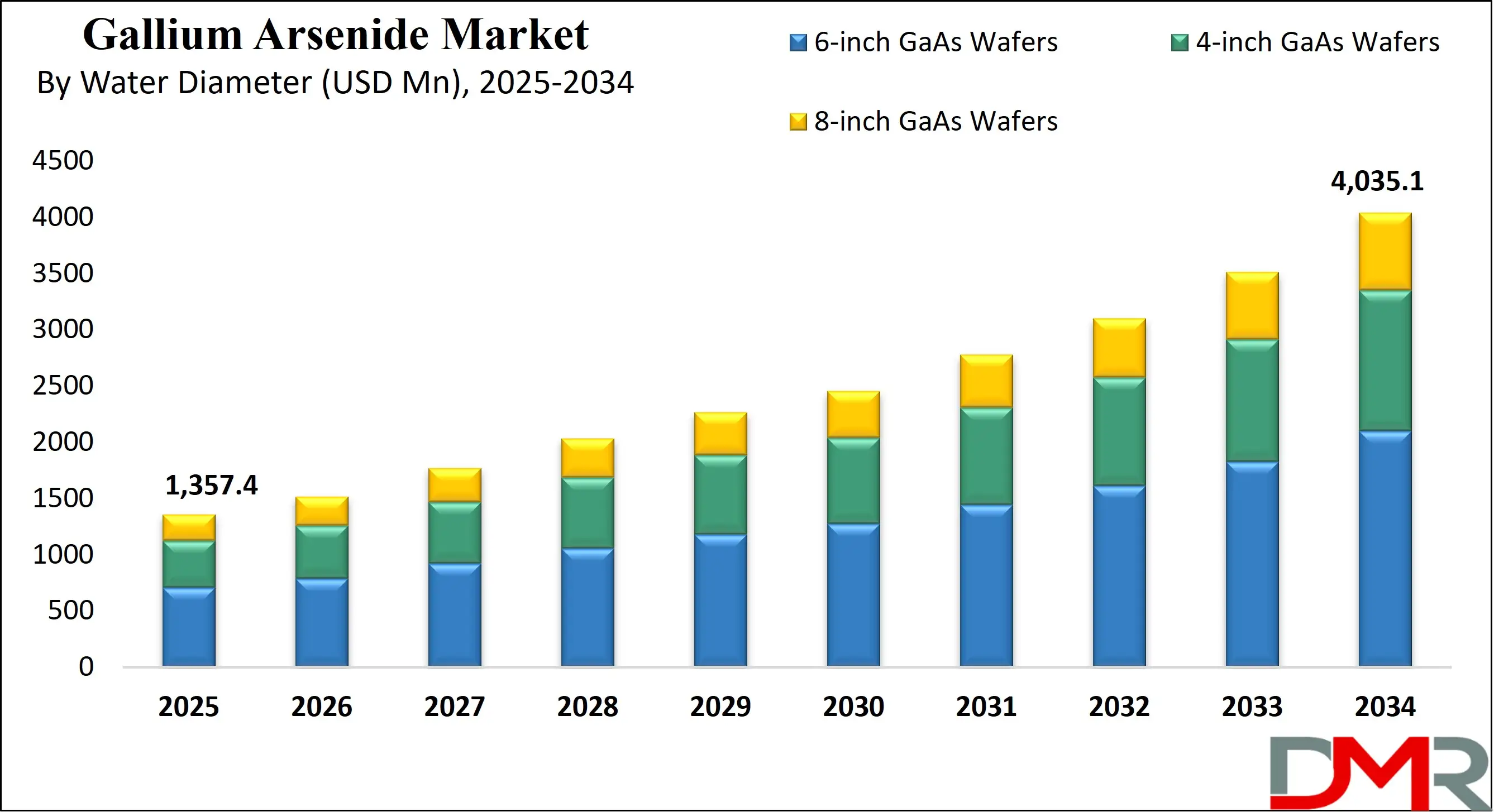
By Water Technology Analysis
6-inch Gallium Arsenide wafers are expected to dominate the wafer diameter segment with a 52.0% share in 2025 due to their balance of cost efficiency, high yield and compatibility with advanced semiconductor fabrication processes. Larger wafer sizes allow manufacturers to produce more devices per wafer, reducing per-unit production costs while maintaining uniformity and quality for RF, microwave and optoelectronic applications. The widespread adoption of 6-inch wafers supports high volume production for 5G infrastructure, satellite communication, defense electronics and high speed data processing, making them the preferred choice for most global GaAs manufacturers.
4-inch Gallium Arsenide wafers, while smaller in size, remain significant in this market segment, particularly for specialized applications and low volume production. They are easier to handle in legacy fabrication equipment and are often used in research, prototyping and niche electronic devices. 4-inch wafers are also suitable for certain optoelectronic components, sensors and power amplifiers where ultra-high throughput is not required, allowing smaller manufacturers and specialized product lines to leverage GaAs technology without investing in larger wafer infrastructure.
By Manufacturing Role Analysis
GaAs wafer manufacturers are expected to dominate the manufacturing role segment with a 49.0% share in 2025 due to their central position in supplying high quality substrates for a wide range of electronic and optoelectronic devices. These manufacturers focus on producing semi-insulating and semi-conducting GaAs wafers with precise crystal quality, uniformity and low defect density, which are essential for RF amplifiers, microwave circuits, laser diodes and photodetectors. Their ability to provide large volumes of consistent wafers supports the growth of telecommunications, aerospace, defense and high speed electronics industries worldwide.
Device manufacturers also play a crucial role in this market segment by converting GaAs wafers into functional electronic components and modules. These companies specialize in fabricating power amplifiers, RF front-end modules, LEDs, laser diodes and high frequency transistors that are integrated into smartphones, 5G networks, satellite systems and optical communication devices. By focusing on device design, packaging and performance optimization, device manufacturers add significant value to the GaAs supply chain and help drive adoption of compound semiconductor technology across diverse industrial applications.
By Application Analysis
RF and microwave devices are expected to dominate the application segment with a 44.0% share in 2025 due to the growing demand for high frequency and high power components in wireless communication, satellite systems, radar and 5G infrastructure. Gallium Arsenide offers superior electron mobility, low signal loss and high thermal stability, making it ideal for power amplifiers, microwave transistors and monolithic microwave integrated circuits. These features enable faster data transmission, improved signal integrity and efficient energy use, which are critical for telecom networks, defense electronics and high speed communication systems worldwide.
Optoelectronics also holds a significant position in this market segment, driven by the rising use of LEDs, laser diodes, photodetectors and VCSELs across consumer electronics, data centers and industrial automation. GaAs based optoelectronic devices provide high light conversion efficiency, precise wavelength control and reliable performance, which are essential for optical communication, display technologies, sensors and advanced lighting solutions. The increasing adoption of these devices in emerging applications such as autonomous vehicles, smart devices and photonics networks continues to support steady growth in the optoelectronics segment.
By End-Use Industry Analysis
Telecommunications are expected to dominate the end-use industry segment with a 41.0% share in 2025 due to the increasing demand for high frequency and high performance components in 5G networks, satellite communication systems and wireless infrastructure. Gallium Arsenide based power amplifiers, RF front-end modules and microwave circuits provide low signal loss, high electron mobility and efficient energy performance, which are critical for maintaining fast data transmission, stable connectivity and reliable network operation. This makes GaAs a preferred material for telecom equipment and infrastructure globally.
Consumer electronics also represent a significant portion of the market, driven by the growing need for smartphones, tablets, wearable devices and other connected electronics that require compact, high efficiency RF and optoelectronic components. GaAs enhances signal quality, data speed and battery efficiency in mobile devices while supporting advanced features such as high frequency communication, optical sensors and miniaturized modules. Increasing adoption of 5G enabled devices and smart electronics continues to expand the use of GaAs in this sector.
The Gallium Arsenide Market Report is segmented on the basis of the following
By Material Type
- Semi-Insulating GaAs
- Semi-Conducting GaAs
By Crystal Growth Technology
- Liquid Encapsulated Czochralski (LEC)
- Vertical Gradient Freeze (VGF)
- Standard VGF
- High-Purity VGF
By Water Diameter
- 6-inch GaAs Wafers
- 4-inch GaAs Wafers
- 8-inch GaAs Wafers
By Manufacturing Role
- GaAs Wafer Manufacturers
- Device Manufacturers
- Foundry & Contract Fabrication
By Application
- RF & Microwave Devices
- Power Amplifiers (Smartphones)
- 5G Infrastructure Equipment
- Radar & Satellite Systems
- Optoelectronics
- LEDs
- Laser Diodes
- VCSELs & Optical Sensors
- Photovoltaic Devices
- Space Solar Cells
- Concentrated Terrestrial PV
- High-Speed & Digital Electronics
By End-Use Industry
- Telecommunications
- Consumer Electronics
- Automotive
- Aerospace & Defense
- Industrial, Research & Others
Global Gallium Arsenide Market: Regional Analysis
Region with the Largest Revenue Share
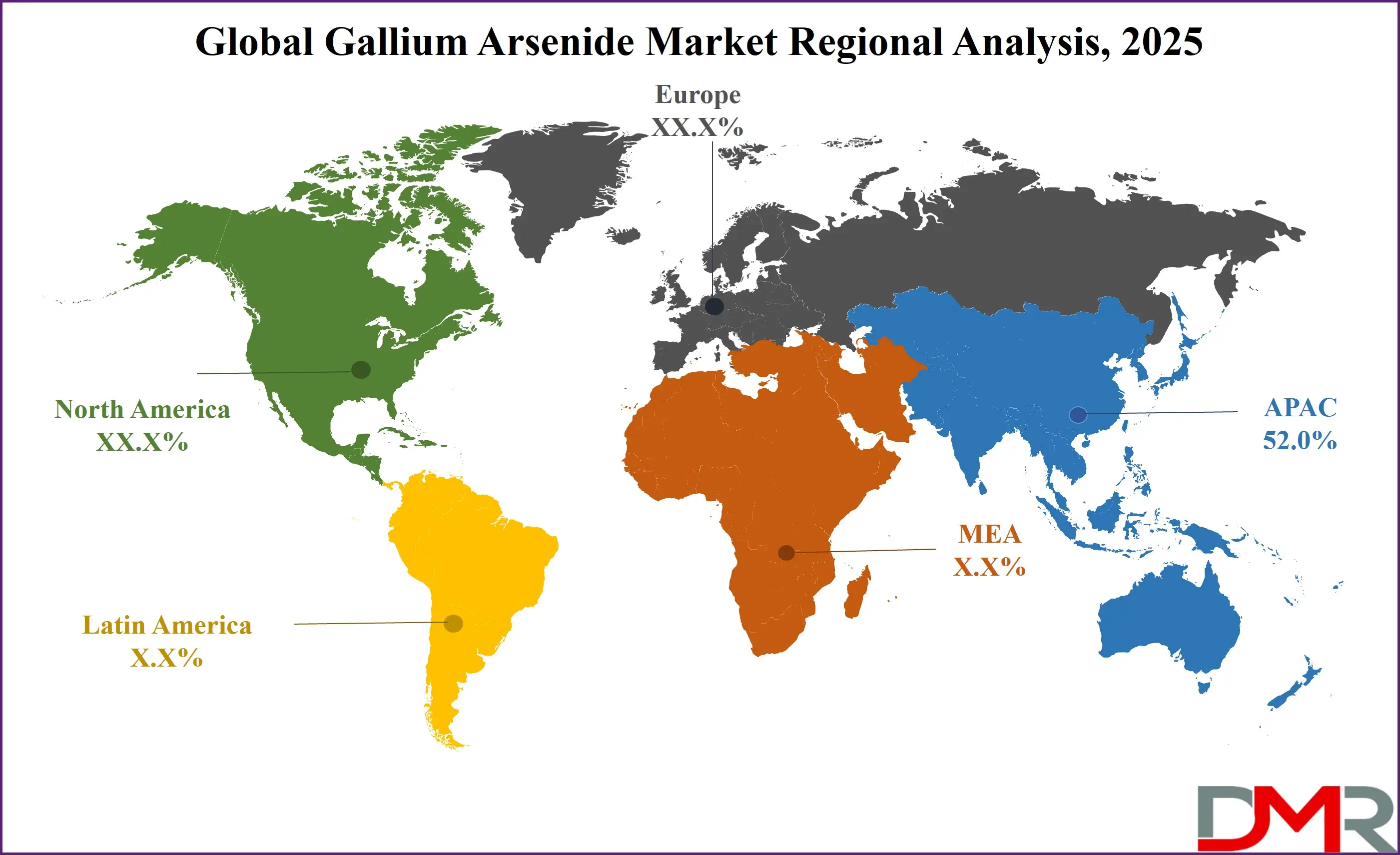
Asia Pacific is expected to lead the global Gallium Arsenide market in 2025, capturing 52.0% of total market revenue, driven by the region’s strong presence in semiconductor manufacturing, telecommunications infrastructure and consumer electronics production. Countries such as China, Japan, South Korea and Taiwan are major hubs for GaAs wafer fabrication, device manufacturing and optoelectronic component production. Rising demand for 5G networks, high speed data communication, satellite systems and advanced electronic devices, along with significant investments in research and development, continues to position Asia Pacific as the largest and fastest growing market for Gallium Arsenide globally.
ℹ
To learn more about this report –
Download Your Free Sample Report Here
Region with significant growth
North America is expected to witness significant growth in the Gallium Arsenide market due to rising investments in 5G infrastructure, defense electronics, aerospace systems and advanced data communication networks. The United States, in particular, drives demand for high performance RF components, microwave devices and optoelectronic modules used in satellite communication, radar systems and high speed networking. Strong government support for semiconductor innovation, increasing adoption of autonomous vehicles and industrial automation, and a mature ecosystem of GaAs wafer and device manufacturers contribute to steady market expansion and make North America a key growth region globally.
By Region
North America
Europe
- Germany
- The U.K.
- France
- Italy
- Russia
- Spain
- Benelux
- Nordic
- Rest of Europe
Asia-Pacific
- China
- Japan
- South Korea
- India
- ANZ
- ASEAN
- Rest of Asia-Pacific
Latin America
- Brazil
- Mexico
- Argentina
- Colombia
- Rest of Latin America
Middle East & Africa
- Saudi Arabia
- UAE
- South Africa
- Israel
- Egypt
- Rest of MEA
Global Gallium Arsenide Market: Competitive Landscape
The global Gallium Arsenide market is highly competitive, characterized by continuous innovation in wafer fabrication, epitaxial growth and device design to meet the rising demand for high frequency, high power and optoelectronic applications. Key players focus on expanding production capacities, improving crystal quality, increasing wafer diameters and optimizing device performance for 5G networks, aerospace systems, consumer electronics and photonics applications. Strategic partnerships, mergers, technological collaborations and investment in research and development are common in the industry, enabling companies to enhance efficiency, reduce costs and maintain a strong position in the rapidly evolving global GaAs market.
Some of the prominent players in the global Gallium Arsenide market are
- Sumitomo Electric Industries
- AXT Inc.
- Freiberger Compound Materials
- IQE plc
- WIN Semiconductors
- IntelliEPI
- Wafer Technology
- Vital Materials
- Xiamen Powerway Advanced Material
- Xinxiang Shenzhou Crystal Technology
- Compound Semiconductor Technologies Global
- LandMark Optoelectronics
- San’an Optoelectronics
- Qingdao Jiaying Semiconductor
- Mitsubishi Chemical Group
- Hitachi Cable Fine Tech
- Wafer Works Corporation
- Skyworks Solutions
- Qorvo
- Broadcom
- Other Key Players
Global Gallium Arsenide Market: Recent Developments
- January 2026: A leading quantum computing firm agreed to acquire a chip manufacturing foundry in a multi‑billion dollar deal to strengthen its semiconductor production and support future compound semiconductor growth.
- January 2026: Shares fell as a pending merger between two RF and mixed‑signal semiconductor suppliers continues toward a combined global entity focused on connectivity and communication markets.
- January 2026: A major semiconductor equipment company introduced advanced thermal‑management solutions compatible with GaAs devices to significantly reduce interface resistance and improve performance in high frequency and RF applications.
- October 2025: A startup completed the design of a GaAs‑based 5G low-noise amplifier front-end chip, marking progress in country‑level RF semiconductor capabilities.
Report Details
| Report Characteristics |
| Market Size (2025) |
USD 1,35.4 Mn |
| Forecast Value (2034) |
USD 4,035.1 Mn |
| CAGR (2025–2034) |
12.9% |
| The US Market Size (2025) |
USD 274.0 Mn |
| Historical Data |
2019 – 2024 |
| Forecast Data |
2026 – 2034 |
| Base Year |
2024 |
| Estimate Year |
2025 |
| Report Coverage |
Market Revenue Estimation, Market Dynamics, Competitive Landscape, Growth Factors, etc. |
| Segments Covered |
Material Type (Semi-Insulating GaAs, Semi-Conducting GaAs) Crystal Growth Technology (Liquid Encapsulated Czochralski (LEC), Vertical Gradient Freeze (VGF)) Wafer Diameter (6-inch GaAs Wafers, 4-inch GaAs Wafers, 8-inch GaAs Wafers) Manufacturing Role (GaAs Wafer Manufacturers, Device Manufacturers, Foundry & Contract Fabrication) Application (RF & Microwave Devices, Optoelectronics, Photovoltaic Devices, High-Speed & Digital Electronics) and End-Use Industry (Telecommunications, Consumer Electronics, Automotive, Aerospace & Defense, Industrial, Research & Others) |
| Regional Coverage |
North America – US, Canada; Europe – Germany, UK, France, Russia, Spain, Italy, Benelux, Nordic, Rest of Europe; Asia-Pacific – China, Japan, South Korea, India, ANZ, ASEAN, Rest of APAC; Latin America – Brazil, Mexico, Argentina, Colombia, Rest of Latin America; Middle East & Africa – Saudi Arabia, UAE, South Africa, Turkey, Egypt, Israel, Rest of MEA |
| Prominent Players |
Sumitomo Electric Industries, AXT Inc., Freiberger Compound Materials, IQE plc, WIN Semiconductors, IntelliEPI, Wafer Technology, Vital Materials, Xiamen Powerway Advanced Material, Xinxiang Shenzhou Crystal Technology, Compound Semiconductor Technologies Global, LandMark Optoelectronics, San’an Optoelectronics, Qingdao Jiaying Semiconductor, and Others. |
| Purchase Options |
We have three licenses to opt for: Single User License (Limited to 1 user), Multi-User License (Up to 5 Users), and Corporate Use License (Unlimited User) along with free report customization equivalent to 0 analyst working days, 3 analysts working days, and 5 analysts working days respectively. |
Frequently Asked Questions
How big is the global Gallium Arsenide market?
▾ The global Gallium Arsenide market size was valued at USD 1,357.4 million in 2025 and is expected to reach USD 4,035.1 million by the end of 2034.
What is the size of the US Gallium Arsenide market?
▾ The US Gallium Arsenide market was valued at USD 274.0 million in 2025. It is expected to witness subsequent growth in the upcoming period as it holds USD 766.4 million in 2034 at a CAGR of 12.1%.
Which region accounted for the largest global Gallium Arsenide market?
▾ Asia Pacific is expected to have the largest market share in the global Gallium Arsenide market, with a share of about 52.0% in 2025.
Who are the key players in the global Gallium Arsenide market?
▾ Some of the major key players in the global Gallium Arsenide market are Sumitomo Electric Industries, AXT Inc., Freiberger Compound Materials, IQE plc, WIN Semiconductors, IntelliEPI, Wafer Technology, Vital Materials, Xiamen Powerway Advanced Material, Xinxiang Shenzhou Crystal Technology, Compound Semiconductor Technologies Global, LandMark Optoelectronics, San’an Optoelectronics, Qingdao Jiaying Semiconductor, and Others.