What is the Semiconductor Materials Market Size?
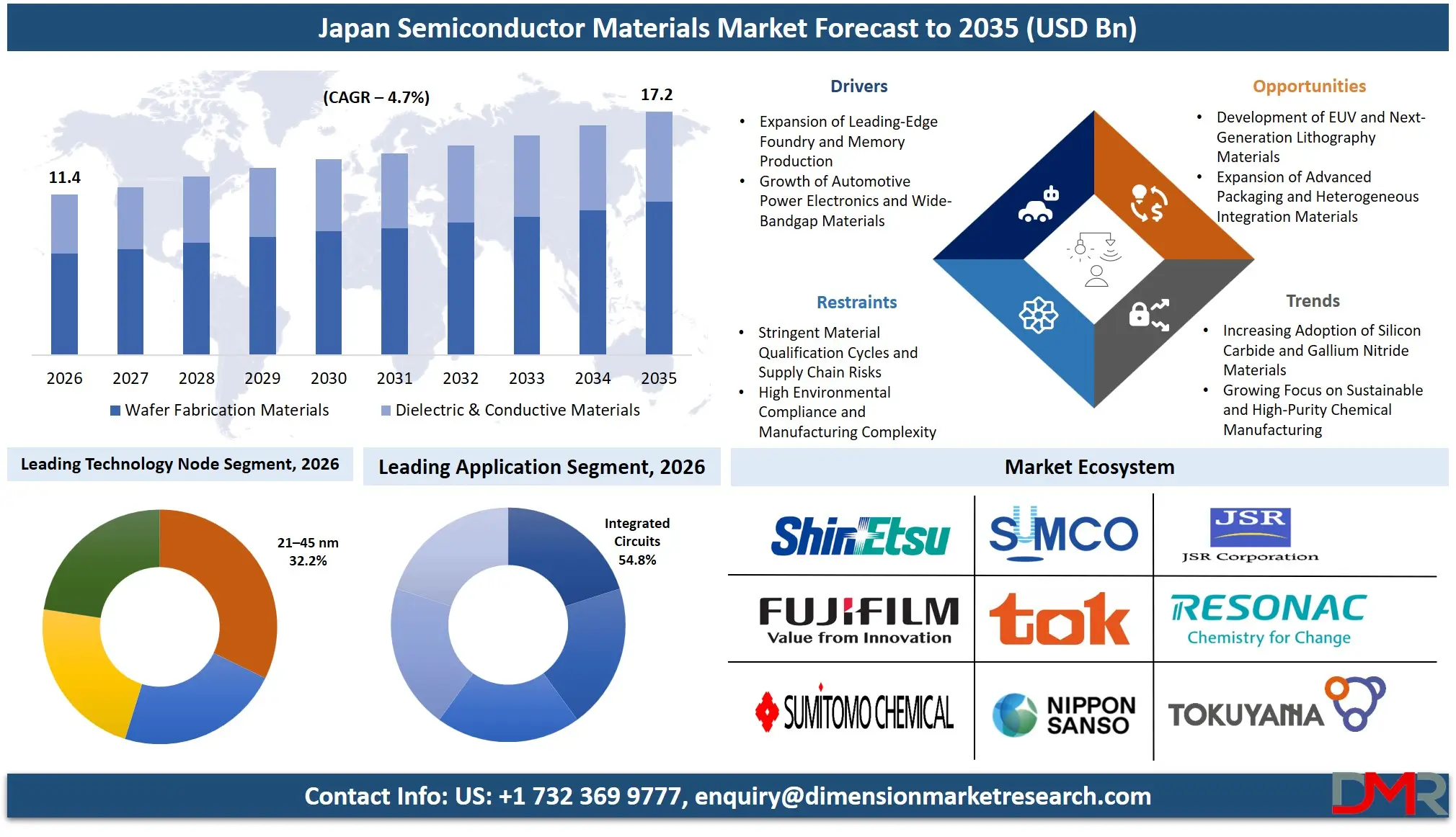
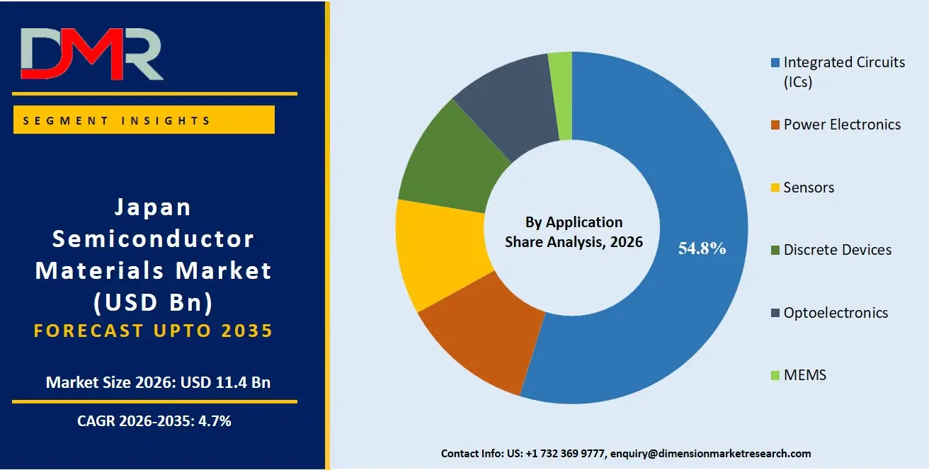
The Japan Semiconductor Materials Market is expected to reach a value of USD 11.4 billion in 2026, and it is further anticipated to reach USD 17.2 billion by 2035, growing at a CAGR of 4.7% during the forecast period.
ℹ
To learn more about this report –
Download Your Free Sample Report Here
The semiconductor materials market has been showing consistent growth due to Japan's rising dependence on resilient, high-performance, and miniaturized electronic systems for effective, secure, and scalable chip production. This includes several material platforms and expert services that help fabs and device manufacturers deploy intelligent solutions for consumer electronics, automotive, and industrial purposes. There has been a rising need for professional services owing to the requirements for implementing advanced wafer fabrication materials, securing operational continuity against supply disruptions, and delivering high-purity chemical delivery systems to customers. Foundry operators have emerged as the largest consumer segment for semiconductor materials services, with silicon wafers being the most popular choice due to their wide availability and reliability, while there has been rapid growth in silicon carbide and gallium nitride platforms.
ℹ
To learn more about this report –
Download Your Free Sample Report Here
Key Takeaways
- Market Size & Forecast: The Japan Semiconductor Materials market is forecasted to be valued at USD 11.4 billion in 2026, growing incrementally to USD 17.2 billion by 2035, due to the joint efforts of technology strategy deployment on the part of enterprises as well as the obligatory deployment of leading-edge and resilient chip technologies.
- Growth Rate & Outlook: Japan market is expected to grow at 4.7% CAGR, propelled by the urgent need to mitigate emerging semiconductor supply chain vulnerabilities, alongside increasing challenges in orchestrating multi-directional material flows from wafer fabrication, packaging, and advanced node production.
- Primary Growth Drivers: Major driving factors comprise the transition from traditional planar transistors towards modern 3D architectures, the necessity to deploy secure and robust supply chains for critical materials, as well as the implementation of advanced process control systems necessitating unique material & services expertise.
- Key Market Trends: Major trends encompass the introduction of AI-driven defect detection for wafer materials through commercial channels, usage of machine learning within wide area networks for material demand forecasting and preventing yield loss, and increased focus on cybersecurity amidst rising supply chain safety considerations of regulators.
- By Material Type Analysis: The Silicon segment is projected to dominate the Japan Semiconductor Materials Market due to strong demand for scalable and efficient wafer substrates supporting real-time process monitoring, line balancing, and performance optimization. Silicon Carbide and Gallium Nitride remain high-growth segments due to power electronics demand.
- By Material Category Analysis: The Wafer Fabrication Materials segment is projected to dominate the market owing to its reliability, large-scale fab connectivity, and widespread use in advanced logic and memory production, industrial infrastructure, and foundry integration.
- By Application Analysis: The Integrated Circuits (ICs) segment is anticipated to lead the Japan Semiconductor Materials Market due to growing deployment of large-scale logic and memory projects supporting fab operations, yield management, and long-term semiconductor production.
What are Semiconductor Materials?
Semiconductor materials are described as substances used to produce chips through wafer fabrication, doping, deposition, and packaging processes. The current generation of semiconductor material systems has incorporated smart features such as purity monitoring systems, inventory management, quality control, and traceability techniques that will allow for the optimization of material usage, distribution, and utilization. This type of material system can be implemented either for logic, memory, power, or analog chips based on the performance needs and available technology node.
Use Cases
- Foundry Yield Resilience: Semiconductor foundries rely on ultra-high-purity materials with strict supplier certification, while fabs handle contamination monitoring and process control internally to ensure yield stability, without materials providers installing detection or automation tools.
- Automotive Power Semiconductor Reliability: Automotive manufacturers rely on silicon carbide (SiC) and gallium nitride (GaN) semiconductor materials to enable high-efficiency, high-temperature, and high-reliability power devices that meet stringent automotive safety and durability standards.
- Industrial and Infrastructure Electronics: Industrial operators and infrastructure systems utilize semiconductor materials in power devices, sensors, and control ICs to ensure stable operation, efficient energy conversion, and reliable performance in harsh environments.
- Manufacturing Supply Chain Optimization: Semiconductor fabs and material suppliers use integrated supply chain planning and traceability systems to ensure the timely delivery of high-purity materials, minimize production disruptions, and maintain consistent wafer manufacturing output.
How AI is Transforming the Semiconductor Materials Market?
AI is revolutionizing the semiconductor materials industry through increased demand forecasting and predictive maintenance capabilities for material production. The analytics platform suite includes AI-based systems that detect consumption anomalies and material inefficiencies in order to resolve them instantaneously, thereby preventing any financial losses and operational damage. In addition, the AI-driven functions of inventory management services help organizations assess material behavior, determine optimal usage schedules, and customize their outage planning. AI forms an essential part of governance and customer trust initiatives. Professional services involve intelligent agents that monitor compliance and keep material quality logs free of any non-compliant entries while ensuring that all operations comply with regulations and the stringent cybersecurity protocols in Japan.
Market Dynamics
Key Drivers in the Japan Semiconductor Materials Market
Expansion of Leading-Edge Foundry and Memory Production
The rapid growth in the manufacture of semiconductors using advanced nodes in Japan has led to a great need for high-purity silicon wafers, EUV photoresists, specialty gases, and CMP slurry products. The leading foundries and memory producers have ramped up capacity for production of logic chips under 5nm technology, 3D NAND chips, and future generations of DRAM that require ultra-high performance in manufacturing processes. There is an increased demand in Japanese semiconductor material suppliers for higher purity chemicals, precursors, and substrate materials, owing to the need for AI, HPC, automotive, and edge chips. The government has also launched several semiconductor localization programs aimed at boosting semiconductor material demand. As Japan plans on enhancing self-sufficiency in chip manufacture, there has been continued demand in wafer fabrication materials, advanced packaging, and specialty substrates.
Growth of Automotive Power Electronics and Wide-Bandgap Materials
The substantial rise in the demand for automotive semiconductors in Japan, especially for electric vehicle power trains, inverters, and chargers, is leading to the use of silicon carbide (SiC) and gallium nitride (GaN). Leading Japanese car manufacturers and Tier-1 suppliers are replacing conventional silicon IGBTs with SiC-based power devices to increase efficiency and performance. As a result, there will be strong demand for SiC epitaxial wafers, GaN on silicon substrates, and other packaging materials such as high-temperature paste for chip attachment, ceramic substrates, and heat-resistant encapsulation resins. Furthermore, the development of renewable energy systems and industrial motors is increasing the usage of SiC and GaN. The government's push for EVs and carbon neutrality will also support this trend for several years in Japan.
Restraints in the Japan Semiconductor Materials Market
Stringent Material Qualification Cycles and Supply Chain Risks
The extensive and meticulous procedures that fab facilities use to qualify new semiconductor materials present substantial logistical problems for both new companies as well as existing suppliers. Fab facilities normally spend around 12–24 months conducting testing and validating the reliability and purity of the new materials in addition to evaluating its lot-to-lot uniformity before certifying the new sources, thereby posing high hurdles to switching suppliers. In addition to this, concerns about geopolitical disruptions along the supply chain, such as export restrictions on specialty chemicals, rare earth metals, and advanced precursor gases, have raised concerns among Japanese material producers who rely on their imports. Costs are also increasing due to expensive fabrication and purification processes. Disruptions of any kind to the raw material supply from supplier regions will cause production delays.
High Environmental Compliance and Manufacturing Complexity
Stringent environmental regulations regarding chemical production and waste management in Japan place heavy operational costs on companies involved in the manufacture of semiconductor materials. Ultra-high-purity processing, solvent recycling facilities, and dangerous substances handling requirements require large investments for semiconductor materials, such as wet chemicals, photoresists, and specialty gases. The new PFAS regulations are especially difficult to follow due to the fact that many semiconductor materials used as surfactants, etchants, and photoresists belong to the substances listed for restriction. This complicates the process for smaller companies that are unable to absorb these costs and compete in prices. Moreover, energy-consuming manufacture of silicon wafers and CMP slurry increases operational costs.
Growth Opportunities in the Japan Semiconductor Materials Market
Development of EUV and Next-Generation Lithography Materials
Growth potential is evident from the development of extreme ultra-violet (EUV) and high numerical aperture (NA) EUV photoresists, underlayers, and patterning materials. The Japanese companies producing chemical and material products are ready to reap their benefits as fabs operate at 2nm and smaller nodes. Metal oxide photoresists, sensitive chemically amplified photoresists, and innovative spin-on carbon masks are demanded due to the need to overcome defects and line-edge roughness issues. In addition, there are demands for photoresist ancillaries such as developer solutions, rinse solutions, and top coat solutions that must be innovated to stay relevant. Leveraging government support programs, such as the LSTC initiative, material suppliers will be able to benefit from supply deals with high margins by qualifying next-generation lithography materials.
Expansion of Advanced Packaging and Heterogeneous Integration Materials
With increased usage of advanced packaging technology solutions in Japan, such as chip-on-wafer-on-substrate (CoWoS), hybrid bonding, and 3D integration, there is a high demand for specialty packaging materials. There is a quick consumption of organic ABF substrates, silicon interposers, die attach film (DAF), NCPs, and wafer-level underfill due to the increasing capacity investment of foundries and OSATs towards heterogeneous integration. Moreover, high heat conductivity TIMs are required to deal with heat dissipation issues in stacked die packages. As more foundries transition from traditional wire bonding to more advanced flip-chip and hybrid bonding approaches, copper hybrid bonding materials and post-bond clean chemicals see increased demand. There is an opportunity for material suppliers in Japan having experience with high-reliability packaging solutions to capitalize on this highly dynamic market.
Trends in the Japan Semiconductor Materials Market
Increasing Adoption of Silicon Carbide and Gallium Nitride Materials
The use of wide-bandgap semiconductors, silicon carbide (SiC) and gallium nitride (GaN), is increasing at an ever-accelerating rate within the Japanese automotive and industrial power device sectors. Power device makers are upgrading their facilities, producing 150 mm SiC chips to 200 mm wafers to lower the cost per chip while increasing their capability in bulk SiC wafer growth and epitaxy. GaN on Silicon (Si) and GaN on sapphire substrates are being used increasingly in fast charging devices, data center power supplies, and 5G base stations. Japanese suppliers have responded to this market trend by scaling up SiC precursor production, high-purity source gas production for GaN film growth, and new Ohmic metal deposition technologies. This momentum is fueled by government subsidies for indigenous wide-bandgap manufacturing and ambitious EV production targets set by Japanese carmakers. The replacement of silicon with SiC/GaN constitutes one of the largest material substitution movements in today's market.
Growing Focus on Sustainable and High-Purity Chemical Manufacturing
One of the most important aspects currently affecting the Japanese semiconductor materials sector is sustainability, which is becoming increasingly significant among leading suppliers who are working on the development of energy-efficient purification technologies and solvent recycling. The drive to adopt innovations related to green chemistry, including the development of environmentally friendly photoresists, is being propelled by environmental regulation and customer demand for low-carbon production chains. Moreover, major fab operators are starting to request from material suppliers data regarding carbon footprints, alongside the adoption of a circular approach towards chemicals packaging. Dry etch and deposition technologies that minimize the emission of greenhouse gases are also becoming more common. By developing environmentally friendly materials that offer high purity and process compatibility, Japanese material suppliers will have a competitive edge.
Research Scope and Analysis
The Japan Semiconductor Materials Market is segmented by material type, material category, technology node, application, and end-use industry. The market supports consumer electronics manufacturing, automotive power management, IT infrastructure, healthcare devices, and industrial automation across individual fabs, foundry operators, public authorities, and electronics companies through cloud-based and on-premise material management solutions.
ℹ
To learn more about this report –
Download Your Free Sample Report Here
By Material Type Analysis
Silicon segment is expected to lead the Japan Semiconductor Materials Market in 2026 with a projected market share of 68.5%, driven by sustained demand for polished and epitaxial wafers from Japan's logic, memory, analog, and discrete device fabs. Japanese silicon wafer suppliers benefit from long-term supply agreements with domestic foundries, IDMs, and memory manufacturers. Silicon Carbide (SiC) and Gallium Nitride (GaN) represent the fastest-growing material types, fueled by automotive EV power train adoption, renewable energy inverters, and industrial power supplies. Gallium Arsenide (GaAs) maintains a stable niche in optoelectronics (laser diodes, LEDs) and high-frequency devices for 5G infrastructure. Indium Phosphide (InP) serves photonic integrated circuits and high-speed communication applications. Sapphire substrates remain relevant for GaN-on-sapphire LED and RF device production.
By Material Category Analysis
Wafer Fabrication Materials are projected to dominate the Japan Semiconductor Materials Market in 2026, with an estimated share of 68.4%, owing to the high volume and value of silicon wafers, photoresists, wet chemicals, CMP slurries, specialty gases, and sputtering targets consumed per wafer start. Japanese fabs performing advanced logic, memory, analog, power, and sensor fabrication require multiple lithography, etch, deposition, and planarization steps, each consuming specific high-purity material. Dielectric & Conductive Materials represent the second-largest category, driven by growing advanced packaging adoption, including fan-out wafer-level packaging (FOWLP), hybrid bonding, and 3D integration. Within packaging, organic substrates (particularly ABF substrates for high-performance processors), copper bonding wires, die attach films (DAFs), non-conductive pastes (NCPs), and underfills are experiencing robust demand from Japan's OSATs and IDM back-end facilities.
By Technology Node Analysis
21–45 nm is projected to hold the largest share of the Japan Semiconductor Materials Market in 2026, with an estimated 32.2%, reflecting Japan's strength in automotive microcontrollers (MCUs), analog ICs, power management ICs, MEMS sensors, and image signal processors that are optimally manufactured on mature and mid-range nodes. Japanese fabs operated by Renesas, Rohm, Sony, and other manufacturers maintain significant production capacity within this node range, supporting sustained demand for semiconductor wafers, photoresists, specialty gases, CMP materials, and deposition materials. The continued expansion of automotive electronics, industrial automation systems, and advanced sensing technologies further reinforces the importance of 21–45 nm process technologies, which offer an optimal balance of performance, reliability, manufacturing efficiency, and cost-effectiveness for a broad range of semiconductor applications in Japan.
By Application Analysis
Integrated Circuits (ICs) are projected to dominate the Japan Semiconductor Materials Market in 2026 with an expected share of 53.3%, driven by production of logic chips (microprocessors, MCUs, SoCs), memory chips (NAND Flash, DRAM), analog ICs, and ASICs. Japanese IC manufacturing consumes the broadest range of materials: silicon wafers, multiple photoresist layers, diverse wet chemicals, CMP slurries for shallow trench isolation and interlayer dielectric planarization, specialty deposition and etch gases, and sputtered metal films. Power Electronics represents the fastest-growing application segment, driven by accelerating adoption of SiC and GaN devices for EVs, charging infrastructure, industrial motor drives, and renewable energy systems. Discrete Devices (diodes, transistors, rectifiers) remain stable, particularly for automotive and industrial use. Sensors (MEMS, CMOS image sensors, magnetic sensors) are significant for Japan, driven by Sony's image sensor fabs and automotive MEMS production. Optoelectronics includes LEDs, laser diodes, and photodetectors for display, lighting, and communication applications.
By End-Use Industry Analysis
Automotive is projected to be the largest end-use industry for the Japan Semiconductor Materials Market in 2026, driven by electrification (EV power trains requiring SiC power devices and high-voltage ICs), advanced driver-assistance systems (ADAS requiring radar, camera sensors, and high-performance SoCs), and vehicle electrification (body controllers, battery management systems, and infotainment). This position is supported by Japan's leadership in automotive MCUs, power semiconductors, sensors, and SiC-based power devices. Consumer Electronics follows as the second-largest segment, encompassing smartphones, gaming consoles, home appliances, and wearable devices.
The Japan Semiconductor Materials Market Report is segmented based on the following:
By Material Type
- Silicon
- Gallium Arsenide
- Silicon Carbide
- Indium Phosphide
- Gallium Nitride
- Sapphire
- Others
By Material Category
- Wafer Fabrication Materials
- Silicon Wafers
- Photoresists
- Photoresist Ancillaries
- Wet Chemicals
- Chemical Mechanical Planarization (CMP) Slurries & Pads
- Gases
- Sputtering Targets
- Dielectric & Conductive Materials
- Packaging Materials
- Lead Frames
- Substrates (Organic, Ceramic)
- Encapsulation Resins
- Bonding Wires
- Die Attach Materials
- Underfills
- Thermal Interface Materials (TIMs)
By Technology Node
- ≤10 nm
- 11–20 nm
- 21–45 nm
- ≥46 nm
By Application
- Integrated Circuits (ICs)
- Discrete Devices
- Optoelectronics
- Sensors
- Power Electronics
- MEMS
By End-Use Industry
- Consumer Electronics
- Automotive
- IT & Telecommunications
- Healthcare
- Industrial
- Defense & Aerospace
- Others
Competitive Landscape
The dynamics of competition in the Japan Semiconductor Materials Market have become increasingly sophisticated, with a diverse mix of global material manufacturers, Japanese chemical companies, wafer suppliers, and specialty material providers competing across wafer fabrication and advanced packaging applications. Success in the market is largely driven by long-term partnerships with semiconductor foundries, integrated device manufacturers (IDMs), memory producers, and assembly and test facilities, enabling suppliers to secure qualified positions within highly demanding semiconductor production processes. Market consolidation continues through strategic acquisitions, joint ventures, and technology collaborations aimed at strengthening capabilities in advanced photoresists, specialty gases, CMP materials, semiconductor substrates, and packaging materials. Proprietary technologies, including ultra-high-purity material processing, advanced chemical formulations, wafer manufacturing expertise, and next-generation packaging materials, have become key competitive differentiators. In addition, consistent product quality, supply chain reliability, technical support, and the ability to meet increasingly stringent performance requirements for advanced nodes and heterogeneous integration architectures remain critical factors shaping competition in the Japanese semiconductor materials industry.
Some of the prominent players in the Japan Semiconductor Materials Market are:
- Shin-Etsu Chemical Co., Ltd.
- SUMCO Corporation
- JSR Corporation
- Tokyo Ohka Kogyo Co., Ltd.
- FUJIFILM Holdings Corporation
- Resonac Holdings Corporation
- Sumitomo Chemical Co., Ltd.
- Mitsubishi Chemical Group Corporation
- Tokuyama Corporation
- Nippon Sanso Holdings Corporation
- Kanto Chemical Co., Inc.
- Stella Chemifa Corporation
- Tri Chemical Laboratories Inc.
- ADEKA Corporation
- Taiyo Holdings Co., Ltd.
- NAMICS Corporation
- Ajinomoto Co., Inc.
- TOPPAN Holdings Inc.
- Osaka Organic Chemical Industry Ltd.
- Toyo Tanso Co., Ltd.
- Other Key Players
Recent Developments
- April 2026: Sumitomo Chemical Co., Ltd. announced the construction of a new Technology Center for advanced semiconductor photoresists at its Osaka Works. The facility will integrate manufacturing process technology management, quality evaluation, and analytical functions to strengthen the company's supply system for EUV and ArF photoresists used in advanced semiconductor manufacturing.
- December 2025: TOPPAN Holdings Inc. announced the installation of a pilot line for advanced semiconductor packaging at its Ishikawa Plant, targeting commissioning in July 2026. The facility will support R&D for glass-based packaging components and organic redistribution layer (RDL) interposers for next-generation AI and high-performance computing semiconductors.
- November 2025: JSR Corporation entered a joint research program with IBM to develop AI-driven semiconductor materials discovery platforms. The collaboration focuses on applying generative AI and advanced data models to accelerate the development of next-generation semiconductor materials and process technologies.
- July 2025: Tokuyama Corporation established OCI Tokuyama Semiconductor Materials Sdn. Bhd., a joint venture with OCI TerraSus in Malaysia for the production and sale of semiconductor-grade polycrystalline silicon semi-finished products. The venture aims to expand supply capacity for advanced semiconductor applications while utilizing clean-energy-based production.
Report Details
| Report Characteristics |
| Market Size (2026) |
USD 11.4 Bn |
| Forecast Value (2035) |
USD 17.2 Bn |
| CAGR (2026–2035) |
4.7% |
| Historical Data |
2021 – 2025 |
| Forecast Data |
2027 – 2035 |
| Base Year |
2025 |
| Estimate Year |
2026 |
| Segments Covered |
By Material Type, Material Category, Technology Node, Application, End-Use Industry |
| Country Coverage |
Japan |
Frequently Asked Questions
How big is the Japan Semiconductor Materials Market?
▾ The Japan Semiconductor Materials Market is poised to be valued at USD 11.4 billion in 2026 and is projected to reach USD 17.2 billion by 2035.
What is the CAGR of the Japan Semiconductor Materials Market from 2026 to 2035?
▾ The market is expected to grow at a CAGR of 4.7% from 2026 to 2035, reflecting the maturing nature of the semiconductor material market and the accelerating complexity of multi-channel, interactive engagement strategies.
What factors are driving the growth of the Japan Semiconductor Materials Market?
▾ Key drivers include the performance imperative for faster, lower-power chips, the need to modernize legacy fab systems, the management complexity of multi-material supply chain orchestration, and the surge in demand for specialty substrates amid evolving EV and AI laws.
What are the major trends in the Japan Semiconductor Materials Market?
▾ Major trends include the integration of AI into demand forecasting and predictive maintenance, the rise of advanced packaging on commercial channels, the demand for vertical-specific analytics solutions, and the focus on secure, cyber-resilient material supply practices.
Who are the key players in the Japan Semiconductor Materials Market?
▾ Key players include Shin-Etsu Chemical, SUMCO Corporation, Tokyo Ohka Kogyo (TOK), and JSR Corporation, alongside Japanese chemical and material infrastructure leaders and many more.
How is the Japan Semiconductor Materials Market segmented?
▾ The market is segmented by material type, material category, technology node, application, and end-use industry.