What is the Japan Semiconductor Production Equipment Market Size?
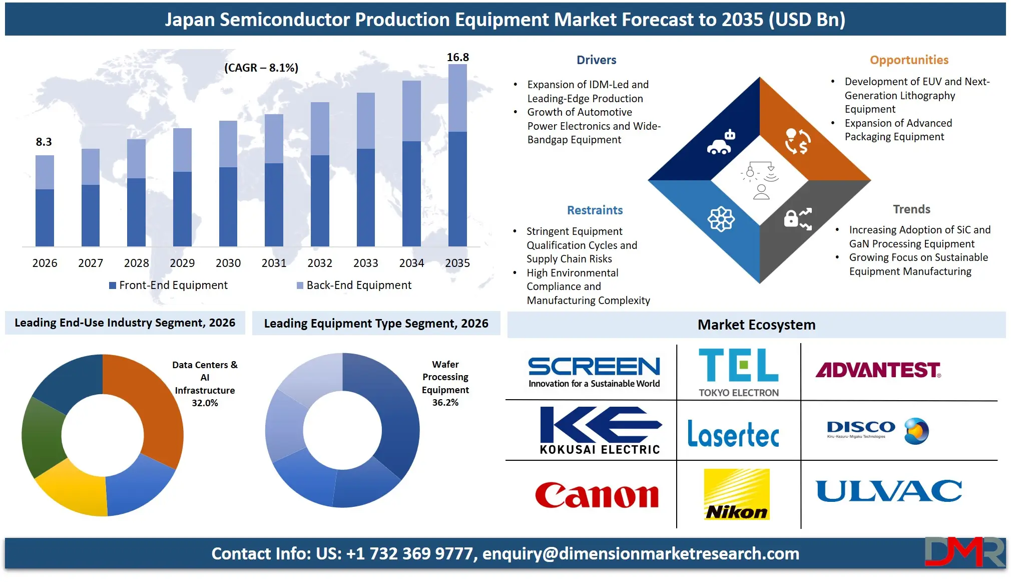
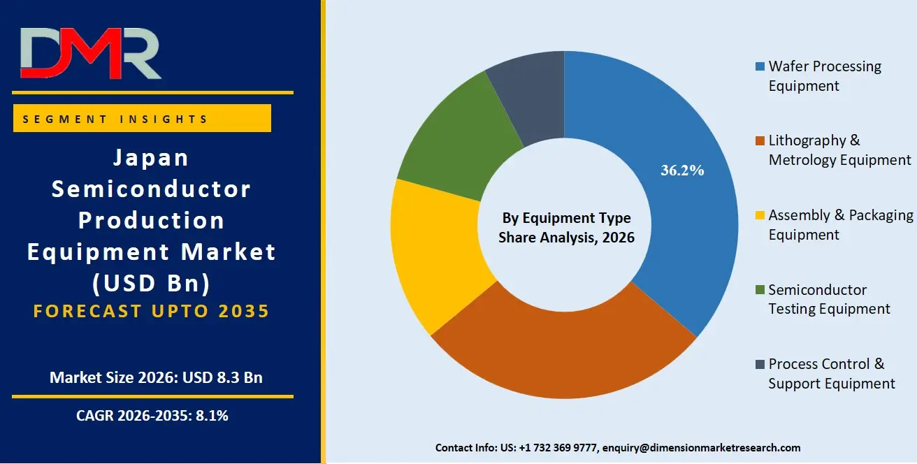
The Japan Semiconductor Production Equipment Market is expected to reach a value of USD 8.3 billion in 2026, and it is further anticipated to reach USD 16.8 billion by 2035, growing at a CAGR of 8.1% during the forecast period.
ℹ
To learn more about this report –
Download Your Free Sample Report Here
The semiconductor production equipment market has been showing consistent growth due to Japan's rising dependence on resilient, high-precision, and miniaturized manufacturing systems for effective, secure, and scalable chip production. This includes several equipment platforms and expert services that help fabs and device manufacturers deploy intelligent solutions for consumer electronics, automotive, and industrial purposes.
There has been a rising need for professional services owing to the requirements for implementing advanced wafer processing tools, securing operational continuity against supply disruptions, and delivering high-uptime equipment support to customers. Integrated device manufacturers (IDMs) such as Renesas, Sony, and Rohm, alongside Japan's equipment export-driven ecosystem, have emerged as the largest consumer segment for semiconductor equipment services, with wafer processing tools being the most popular choice due to their critical role in chip fabrication, while there has been rapid growth in assembly & packaging and testing equipment platforms.
ℹ
To learn more about this report –
Download Your Free Sample Report Here
Key Takeaways
- Market Size & Forecast: The Japan Semiconductor Production Equipment market is forecasted to be valued at USD 8.3 billion in 2026, growing incrementally to USD 16.8 billion by 2035, due to the joint efforts of technology strategy deployment on the part of enterprises as well as the obligatory deployment of leading-edge and resilient chip manufacturing technologies.
- Growth Rate & Outlook: Japan market is expected to grow at 8.1% CAGR, propelled by the urgent need to mitigate emerging semiconductor supply chain vulnerabilities, alongside increasing challenges in orchestrating multi-directional equipment flows from wafer fabrication, assembly, packaging, and testing.
- Primary Growth Drivers: Major driving factors comprise the transition from traditional planar transistors towards modern 3D architectures, the necessity to deploy secure and robust supply chains for critical production tools, as well as the implementation of advanced process control systems necessitating unique equipment & services expertise.
- Key Market Trends: Major trends encompass the introduction of AI-driven predictive maintenance for wafer processing equipment, the usage of machine learning for equipment demand forecasting, and increased focus on supply chain resilience amidst rising fab safety considerations of regulators.
- By Production Phase Analysis: The Front-End Equipment segment is projected to dominate the Japan Semiconductor Production Equipment Market due to strong demand for scalable and efficient wafer processing systems. Back-End Equipment remains a high-growth segment due to advanced packaging demand.
- By Equipment Type Analysis: The Wafer Processing Equipment segment is projected to dominate the market owing to its large-scale fab integration and widespread use in IDM-led logic and memory production. Lithography & Metrology Equipment follows closely, driven by EUV adoption.
- By Chip Application Analysis: The Logic Devices segment is anticipated to lead the Japan Semiconductor Production Equipment Market due to growing deployment of large-scale logic projects supporting fab operations, yield management, and long-term semiconductor production.
What is Semiconductor Production Equipment?
Semiconductor production equipment refers to machines and tools used to produce chips through wafer fabrication, lithography, etching, deposition, assembly, packaging and testing processes. The current generation of semiconductor equipment systems incorporates smart features including real-time sensors, quality control modules and traceability techniques for tool optimisation. This type of equipment system can be implemented for logic, memory, or power device production based on the performance needs and available technology node.
Use Cases
- Foundry Yield Resilience: Semiconductor foundries have ultra-precise wafer processing equipment with strict supplier certification. Fabs manage contamination monitoring and process control in-house to ensure yield stability.
- Automotive Power Semiconductor Reliability: High-efficiency, high-temperature and high-reliability power device manufacturing requires advanced silicon carbide (SiC) and gallium nitride (GaN) production equipment from automotive manufacturers.
- Industrial and Infrastructure Electronics: Semiconductor production equipment for power devices, sensors and control ICs for stable operation and energy efficient conversion for industrial operators.
- Manufacturing Supply Chain Optimization: Integrated supply chain planning systems allow semiconductor fabs and equipment suppliers to guarantee on-time delivery of high-precision tools and consistent output.
How AI is Transforming the Semiconductor Production Equipment Market?
AI is transforming Japan's semiconductor production equipment market through three specific, high-impact applications. First, predictive chamber matching. AI models analyze thousands of real-time sensor parameters from Tokyo Electron and Kokusai Electric etch and deposition tools to predict when process chambers will drift out of specification, enabling proactive recalibration before yield loss occurs. Second, virtual metrology. Rather than measuring every wafer, AI infers critical dimension and film thickness from equipment sensor data, reducing measurement cycle time by 60 to 80 percent in Japanese fabs. Third, adaptive recipe optimization. Machine learning algorithms adjust lithography focus, etch time, and deposition parameters across Nikon scanners and TEL etchers based on real-time wafer state, compensating for upstream variations. Japanese equipment suppliers are also deploying AI for anomaly detection in ultra-high vacuum systems and predictive part replacement for consumables like RF generators and electrostatic chucks. These capabilities have shifted equipment value from raw throughput to AI driven uptime and process stability, particularly critical for Japan's IDM led automotive and power semiconductor production.
Market Dynamics
Key Drivers in the Japan Semiconductor Production Equipment Market
Expansion of IDM-Led and Leading-Edge Production
The rapid growth in semiconductor manufacturing using advanced nodes in Japan, led by IDMs such as Renesas, Sony, and Kioxia, has created strong demand for high-precision wafer processing tools, EUV lithography systems, and etching equipment. Japanese IDMs and memory producers have ramped up capacity for logic chips under 5nm technology, 3D NAND, and next-generation DRAM. The government has also launched several semiconductor localization programs aimed at boosting domestic equipment demand. As Japan plans on enhancing self-sufficiency in chip manufacture, there has been continued demand for front-end tools, advanced packaging equipment, and specialty testers.
Growth of Automotive Power Electronics and Wide-Bandgap Equipment
The substantial rise in automotive semiconductor production in Japan, especially for electric vehicle power trains and inverters, is driving deployment of specialized equipment for silicon carbide (SiC) and gallium nitride (GaN). Japanese car manufacturers and Tier-1 suppliers are increasing adoption of SiC-based power devices. As a result, there will be strong demand for SiC epitaxial deposition systems, GaN-on-silicon processing tools, and high-temperature die attach equipment. The government's push for EVs and carbon neutrality will support this trend for several years.
Restraints in the Japan Semiconductor Production Equipment Market
Stringent Equipment Qualification Cycles and Supply Chain Risks
Fab facilities normally spend around 12 to 24 months qualifying new semiconductor production equipment, posing high hurdles to switching suppliers. This lengthy process involves extensive wafer testing, process matching to existing tools, and reliability validation across multiple lots. Japanese IDMs such as Renesas, Sony, and Rohm require strict adherence to their proprietary process baselines before approving new equipment sources. Geopolitical concerns, particularly export restrictions on advanced lithography and etch tools from foreign jurisdictions, have raised supply chain anxieties among Japanese equipment users. Domestic fabs worry about sudden denial of service or spare parts for critical imported tools. Costs are also increasing due to expensive research and development for next generation platforms and complex manufacturing processes. Smaller Japanese equipment suppliers struggle to maintain competitiveness against larger global players with deeper R&D budgets.
High Environmental Compliance and Manufacturing Complexity
Stringent environmental regulations in Japan place high operational costs on semiconductor equipment manufacturers. The Japanese government enforces rigorous standards for chemical handling, waste treatment, and emissions control at production facilities. PFAS regulations directly affect equipment components, including seals, gaskets, coolants, and specialty O-rings used in vacuum chambers and gas delivery systems. Compliance requires extensive documentation, material substitution, and requalification of affected parts. Energy-consuming operation of wafer processing tools such as etchers, deposition systems, and thermal processing chambers also increases operational costs for equipment manufacturers. These tools run continuously in cleanroom environments requiring massive HVAC and exhaust systems. Smaller equipment vendors face disproportionate compliance burdens, lacking dedicated environmental engineering teams. This creates barriers to entry and favors large, well-capitalized suppliers in the Japanese market.
Growth Opportunities in the Japan Semiconductor Production Equipment Market
Development of EUV and Next-Generation Lithography Equipment
Growth potential exists for high numerical aperture EUV lithography tools, advanced overlay metrology systems, and defect inspection platforms as Japanese fabs move to 2 nanometer nodes and below. Japanese companies producing precision optics, ultra smooth mirrors, and high stability stages are well positioned to supply critical subsystems. Nikon and Canon continue developing domestic lithography alternatives despite global competition. Government support programs such as the Leading edge Semiconductor Technology Center (LSTC) initiative provide funding and collaborative frameworks for next generation lithography development. Japanese material suppliers also benefit because new lithography tools require novel photoresists, pellicles, and underlayers. The shift from deep ultraviolet to EUV and high NA EUV creates replacement cycles for legacy equipment. Domestic suppliers of wafer handlers, reticle stages, and vacuum components can secure long term supply agreements with lithography tool integrators.
Expansion of Advanced Packaging Equipment
With increased adoption of chip on wafer on substrate (CoWoS), hybrid bonding, and 3D integration in Japan, demand is rising for wafer level bonding systems, high precision die attach tools, and compression molding machines. Japanese IDMs and OSATs are investing in back end capacity to support heterogeneous integration for AI and high performance computing applications. As more manufacturers transition from wire bonding to hybrid bonding, bonders and post bond cleaning systems see significantly increased demand. Disco Corporation and Shibaura Mechatronics lead in dicing, grinding, and bonding solutions for advanced packages. The shift from traditional flip chip to copper hybrid bonding requires sub micron alignment accuracy and room temperature bonding capabilities. Japanese equipment suppliers with experience in high reliability packaging for automotive and industrial applications can capitalize on this dynamic market segment, particularly as domestic chip production expands.
Trends in the Japan Semiconductor Production Equipment Market
Increasing Adoption of SiC and GaN Processing Equipment
Wide bandgap semiconductor production equipment is accelerating rapidly in Japanese automotive and industrial power device sectors. Power device makers such as Rohm, Mitsubishi Electric, and Fuji Electric are upgrading from 150 millimeter to 200 millimeter silicon carbide production lines to lower per chip costs. Japanese suppliers are scaling up specialized equipment including high temperature implanters capable of processing silicon carbide at 500 degrees Celsius or higher, high temperature annealing systems exceeding 1,800 degrees Celsius, and ohmic contact deposition tools for nickel and titanium aluminide films. Government subsidies for domestic wide bandgap manufacturing further fuel this momentum. The transition from silicon to silicon carbide and gallium nitride represents one of the largest equipment substitution opportunities in the power semiconductor market. Japanese auto makers including Toyota, Honda, and Nissan are driving demand for electric vehicle power trains requiring these advanced manufacturing tools.
Growing Focus on Sustainable Equipment Manufacturing
Sustainability is driving development of energy efficient processing chambers and exhaust abatement systems across Japan's semiconductor equipment industry. Major fab operators including Kioxia, Micron Japan, and TSMC Japan are requesting detailed carbon footprint data from their equipment suppliers as part of procurement decisions. Dry etch and deposition tools with reduced perfluorocompound and greenhouse gas emissions are becoming standard requirements rather than optional features. Tokyo Electron and Kokusai Electric have introduced chamber cleaning technologies that reduce global warming potential by up to 80 percent compared to previous generations. Japanese equipment manufacturers are also designing tools for easier component recycling and reduced consumable waste. Factory automation systems now track energy consumption per wafer processed. These sustainability trends are no longer marketing differentiators but competitive requirements for selling into Japan's environmentally conscious semiconductor fabs.
Research Scope and Analysis
The Japan Semiconductor Production Equipment Market is segmented by production phase, equipment type, technology node, chip application, and end-use industry. The market supports consumer electronics manufacturing, automotive power management, IT infrastructure, healthcare devices, and industrial automation across individual fabs, foundry operators, public authorities, and electronics companies through cloud-based and on-premise equipment management solutions.
ℹ
To learn more about this report –
Download Your Free Sample Report Here
By Production Phase Analysis
Front-End Equipment segment is expected to lead the Japan Semiconductor Production Equipment Market in 2026 with a projected market share of 63.3%, driven by sustained demand for wafer processing, lithography, etch, deposition, and metrology tools from Japan's logic, memory, analog, and discrete device fabs. Japanese equipment users benefit from long-term service agreements with domestic foundries, IDMs, and memory manufacturers. Back-End Equipment represents the fastest-growing production phase, fueled by automotive EV power train adoption, renewable energy inverters, and industrial power supplies, as well as advanced packaging adoption.
By Equipment Type Analysis
Wafer Processing Equipment is projected to dominate the Japan Semiconductor Production Equipment Market in 2026, with an estimated share of 36.2%, owing to the high volume and value of etchers, deposition tools, clean systems, and thermal processing equipment consumed per wafer start. Japanese fabs performing advanced logic, memory, analog, power, and sensor fabrication require multiple lithography, etch, deposition, and planarization steps, each consuming specific high-precision equipment. Assembly & Packaging Equipment represents the second-largest category, driven by growing advanced packaging adoption, including fan-out wafer-level packaging (FOWLP), hybrid bonding, and 3D integration. Within packaging, wafer-level bonders, die attach systems, compression molders, and singulation tools are experiencing robust demand from Japan's OSATs and IDM back-end facilities.
By Technology Node Analysis
Mid Nodes (21–45 nm equivalent) is projected to hold the largest share of the Japan Semiconductor Production Equipment Market in 2026, with an estimated 32.2%, reflecting Japan's strength in automotive microcontrollers (MCUs), analog ICs, power management ICs, MEMS sensors, and image signal processors that are optimally manufactured on mature and mid-range equipment. Japanese fabs operated by Renesas, Rohm, Sony, and other manufacturers maintain significant production capacity within this node range, supporting sustained demand for wafer processing tools, lithography systems, etching and deposition equipment, and inspection systems. The continued expansion of automotive electronics, industrial automation systems, and advanced sensing technologies further reinforces the importance of mid-node process equipment, which offers an optimal balance of performance, reliability, manufacturing efficiency, and cost-effectiveness for a broad range of semiconductor applications in Japan.
By Chip Application Analysis
Logic Devices are projected to dominate the Japan Semiconductor Production Equipment Market in 2026 with an expected share of 53.3%, driven by production of microprocessors, MCUs, SoCs, and ASICs. Japanese logic device manufacturing consumes the broadest range of equipment: wafer processing tools, multiple lithography systems, diverse etch and deposition chambers, CMP planarizers, and inspection and metrology tools. Analog, Power & Discrete Devices represents the fastest-growing chip application segment, driven by accelerating adoption of SiC and GaN devices for EVs, charging infrastructure, industrial motor drives, and renewable energy systems. Memory Devices (NAND Flash, DRAM) remain stable, particularly for data center and AI infrastructure. Sensors (MEMS, CMOS image sensors) are significant for Japan, driven by Sony's image sensor fabs and automotive MEMS production.
By End-Use Industry Analysis
Data Centers & AI Infrastructure is projected to be the largest end-use industry for the Japan Semiconductor Production Equipment Market in 2026, accounting for 32.0% share, driven by electrification of high-performance computing (AI accelerators and GPUs requiring advanced node production tools and high-bandwidth memory manufacturing equipment), advanced driver-assistance systems (ADAS requiring radar, camera sensors, and high-performance SoC lines), and next-generation computing demand (logic, memory, and heterogeneous integration). This position is supported by rising demand for advanced wafer fabrication equipment, EUV lithography systems, and advanced packaging tools such as 2.5D and 3D integration platforms. Consumer Electronics follows as a leading segment, encompassing smartphones, gaming consoles, home appliances, and wearable devices.
The Japan Semiconductor Production Equipment Market Report is segmented based on the following:
By Production Phase
- Front-End Equipment
- Back-End Equipment
By Equipment Type
- Wafer Processing Equipment
- Lithography & Metrology Equipment
- Assembly & Packaging Equipment
- Semiconductor Testing Equipment
- Process Control & Support Equipment
By Technology Node
- Mature Nodes
- Mid Nodes
- Advanced Nodes
- Leading Edge Nodes
By Chip Application
- Logic Devices
- Memory Devices
- Analog, Power & Discrete Devices
By End-Use Industry
- Consumer Electronics
- Automotive
- Data Centers & AI Infrastructure
- Industrial & Manufacturing
- Telecommunications
Competitive Landscape
The dynamics of competition in the Japan Semiconductor Production Equipment Market have become increasingly sophisticated, with a diverse mix of global equipment manufacturers, Japanese precision engineering companies, wafer processing tool suppliers, and specialty equipment providers competing across front-end and back-end applications. Success in the market is largely driven by long-term partnerships with semiconductor foundries, integrated device manufacturers (IDMs), memory producers, and assembly and test facilities, enabling suppliers to secure qualified positions within highly demanding semiconductor production processes. Market consolidation continues through strategic acquisitions, joint ventures, and technology collaborations aimed at strengthening capabilities in advanced lithography, etch, deposition, inspection, assembly, and test equipment. Proprietary technologies, including ultra-high-precision motion control, advanced plasma sources, high-throughput automation, and next-generation hybrid bonding tools, have become key competitive differentiators. In addition, consistent equipment uptime, supply chain reliability, technical support, and the ability to meet increasingly stringent performance requirements for advanced nodes and heterogeneous integration architectures remain critical factors shaping competition in the Japanese semiconductor production equipment industry.
Some of the prominent players in the Japan Semiconductor Production Equipment Market are:
- Tokyo Electron Limited
- SCREEN Holdings Co., Ltd.
- Advantest Corporation
- KOKUSAI Electric Corporation
- Disco Corporation
- ULVAC, Inc.
- Nikon Corporation
- Canon Inc.
- Hitachi High-Tech Corporation
- Lasertec Corporation
- Tokyo Seimitsu Co., Ltd.
- TOWA Corporation
- Nissin Ion Equipment Co., Ltd.
- Ferrotec Holdings Corporation
- HORIBA, Ltd.
- JEOL Ltd.
- ASML Holding N.V.
- Applied Materials, Inc.
- Lam Research Corporation
- KLA Corporation
- Other Key Players
Recent Developments
- January 2026: ASML Holding N.V. confirmed expanded deployment of High-NA EUV lithography systems for next-generation semiconductor manufacturing, with pilot production tools being installed at leading-edge logic fabs targeting sub-2nm node development, marking a key transition phase in advanced lithography scaling.
- December 2025: KOKUSAI ELECTRIC Corporation showcased advanced batch atomic layer deposition (ALD) and thermal processing systems at SEMICON Japan 2025, emphasizing next-generation film deposition technologies for logic and memory scaling and improved manufacturing efficiency.
- December 2025: Tokyo Seimitsu Co., Ltd., and Advantest Corporation announced a joint development program for a new die-level prober designed for advanced semiconductor testing of AI and high-performance computing devices using 2.5D/3D packaging architectures.
- April 2025: Tokyo Electron Limited and IBM extended their long-term joint research collaboration focused on next-generation semiconductor process technologies, including advanced patterning, 3D chip stacking, and High-NA EUV-era device architectures to support AI and HPC chip scaling beyond 2nm nodes.
Report Details
| Report Characteristics |
| Market Size (2026) |
USD 8.3 Bn |
| Forecast Value (2035) |
USD 16.8 Bn |
| CAGR (2026–2035) |
8.1% |
| Historical Data |
2021 – 2025 |
| Forecast Data |
2027 – 2035 |
| Base Year |
2025 |
| Estimate Year |
2026 |
| Segments Covered |
By Production Phase, By Equipment Type, By Technology Node, By Chip Application, By End-Use Industry |
| Country Coverage |
Japan |
Frequently Asked Questions
How big is the Japan Semiconductor Production Equipment Market?
▾ The Japan Semiconductor Production Equipment Market is poised to be valued at USD 8.3 billion in 2026 and is projected to reach USD 16.8 billion by 2035.
What is the CAGR of the Japan Semiconductor Production Equipment Market from 2026 to 2035?
▾ The market is projected to grow at a CAGR of around 8.1% from 2026 to 2035, reflecting the maturing nature of the semiconductor equipment market and the accelerating complexity of multi-channel, interactive engagement strategies.
What factors are driving the growth of the Japan Semiconductor Production Equipment Market?
▾ Key drivers include the performance imperative for faster, lower-power chips, the need to modernize legacy fab systems, the management complexity of multi-equipment supply chain orchestration, and the surge in demand for specialty substrates and their associated processing tools amid evolving EV and AI laws.
What are the major trends in the Japan Semiconductor Production Equipment Market?
▾ Major trends include the integration of AI into predictive maintenance and demand forecasting, the rise of advanced packaging equipment on commercial channels, the demand for vertical-specific analytics solutions, and the focus on secure, cyber-resilient equipment supply practices.
Who are the key players in the Japan Semiconductor Production Equipment Market?
▾ Key players include Tokyo Electron Limited (TEL), Advantest Corporation, Disco Corporation, SCREEN Holdings, and Nikon Corporation, alongside Japanese precision engineering and test infrastructure leaders and many more.
How is the Japan Semiconductor Production Equipment Market segmented?
▾ The market is segmented by production phase, equipment type, technology node, chip application, and end-use industry.