What is the Photosensitive Semiconductor Device Market Size?
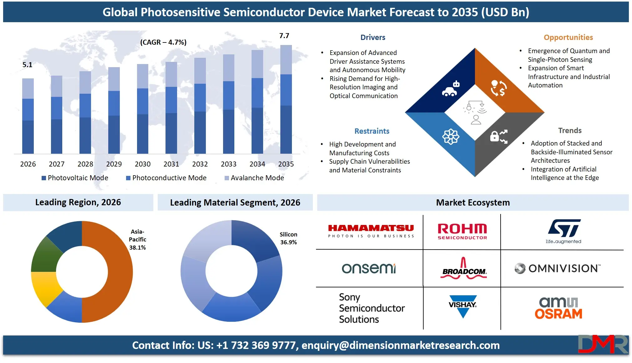
The Global Photosensitive Semiconductor Device Market is expected to reach a value of USD 5.1 billion in 2026, and it is further anticipated to reach USD 7.7 billion by 2035, growing at a CAGR of 4.7% during the forecast period.
ℹ
To learn more about this report –
Download Your Free Sample Report Here
The photosensitive semiconductor device market is experiencing steady growth, propelled by the proliferation of automation, smart sensing, and high-speed optical communication. This market encompasses a range of components—including CMOS image sensors, photodiodes, and phototransistors—that convert light into electrical signals. These devices are foundational to modern electronics, enabling machine vision, advanced driver-assistance systems (ADAS), and high-speed data transmission. The accelerating deployment of LiDAR in autonomous vehicles, the expansion of data center interconnects, and the integration of sophisticated imaging in smartphones and medical equipment are key factors fueling the demand for specialized, high-performance photosensitive devices. Industries such as consumer electronics, automotive, and healthcare are primary drivers, requiring solutions that offer higher resolution, greater spectral sensitivity, and faster response times.
The US Photosensitive Semiconductor Device Market
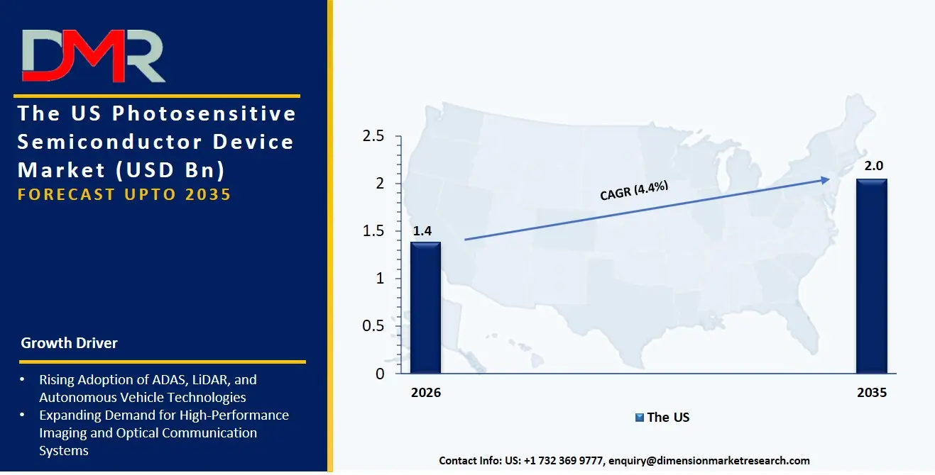
The US Photosensitive Semiconductor Device Market is projected to reach USD 1.4 billion in 2026 and is further expected to grow to USD 2.0 billion by 2035 at a CAGR of 4.4%. The United States remains a central hub for innovation, driven by substantial investment in autonomous vehicle development and advanced research instrumentation.
ℹ
To learn more about this report –
Download Your Free Sample Report Here
The market is characterized by high demand for Avalanche Photodiodes and SPADs, which are critical components in long-range LiDAR systems and quantum sensing applications. Furthermore, the ongoing expansion of hyperscale data centers is generating significant demand for high-speed Indium Gallium Arsenide (InGaAs) photodiodes used in optical transceivers, underscoring the market's shift towards Near-Infrared (NIR) and Infrared (IR) spectral solutions.
The Europe Photosensitive Semiconductor Device Market
The Europe Photosensitive Semiconductor Device Market is estimated to be valued at USD 1.2 billion in 2026 and is further anticipated to reach USD 1.8 billion by 2035 at a CAGR of 4.6%. The European market is significantly shaped by stringent automotive safety regulations and a world-leading industrial automation base. The mandate for advanced driver-assistance systems (ADAS) in new vehicles is a powerful catalyst for CMOS image sensors and photodiodes designed for in-cabin and external monitoring. The region's strong emphasis on "Industry 4.0" is driving demand for robust machine vision systems utilizing BSI and stacked sensor technologies for quality control and robotic guidance. Additionally, scientific research initiatives, particularly in astronomy and particle physics, create a specialized demand for SPAD/QIS and high-purity Germanium photodetectors for astronomical detectors and laboratory analytical instruments.
The Japan Photosensitive Semiconductor Device Market
The Japan Photosensitive Semiconductor Device Market is projected to be valued at USD 431.1 million in 2026 at a CAGR of 4.2%. Japan's market is characterized by its precision manufacturing heritage and leadership in optical components. A key driver is the convergence of its automotive and electronics industries, focusing on the development of compact, highly reliable In-Cabin Monitoring Systems and next-generation LiDAR. Japanese firms are deeply involved in the material science of Indium Gallium Arsenide (InGaAs) and Silicon photonics, propelling advancements in optical communication and datacom applications. The market also sees a unique demand for Photo ICs, which integrate photosensitive elements with signal processing circuitry to provide highly efficient, miniaturized solutions for industrial automation and robotics in factory settings.
Key Takeaways
- Market Size & Forecast: The Global Photosensitive Semiconductor Device market is projected to be valued at USD 5.1 billion in 2026 and reach USD 7.7 billion by 2035, fueled by the pervasive integration of visual and photonic sensing across automotive, industrial, and communication sectors.
- Growth Rate & Outlook: Global market growth is expected at a steady CAGR of 4.7%, sustained by the increasing sophistication of ADAS platforms and the relentless bandwidth demands of data center interconnects.
- Primary Growth Drivers: Key forces include the automotive industry's transition toward autonomous driving via LiDAR and ADAS cameras, the deployment of Industry 4.0 solutions requiring advanced machine vision, and the global rollout of fiber-optic infrastructure.
- Key Market Trends: Major trends include the evolution of 3D sensing via SPAD/QIS and stacked sensor architectures, a pivot toward NIR/IR spectral response for LiDAR and biometrics, and the integration of on-device AI processing with Photo ICs for smart decision-making at the edge.
- By Device Type Analysis: CMOS Image Sensors, particularly advanced BSI and Stacked Sensors, are expected to dominate market revenue due to their ubiquity in smartphones, automotive cameras, and industrial vision systems.
- By Spectral Response Analysis: While the visible spectrum currently leads, Near-Infrared (NIR) and Infrared (IR) are the fastest-growing segments, driven by LiDAR, optical transceivers, and biometric recognition systems like facial authentication.
- By Application Analysis: Consumer Electronics is poised to dominate as the most lucrative application segment, propelled by the exponential increase in per-vehicle sensor content for ADAS, LiDAR, and in-cabin monitoring.
- Regional Leadership: Asia-Pacific is poised to command the largest market share at 38.1% in 2026, driven by its massive consumer electronics manufacturing base and a rapidly advancing automotive production ecosystem.
What is the Photosensitive Semiconductor Device?
Photosensitive Semiconductor Devices are specialized electronic components manufactured from materials like Silicon, GaAs, and InGaAs that detect and respond to light across Ultraviolet, Visible, Near-Infrared, and Infrared spectrums. This market encompasses the design, fabrication, and integration of these devices, which range from complex CMOS Image Sensors with millions of pixels to single-element photodiodes. The technology operates in various modes—photovoltaic, photoconductive, and avalanche—to convert photons into measurable electrical current for imaging, detection, and communication. As industries embed intelligence into their products, these devices have become critical for bridging the physical and digital worlds, enabling applications from smartphone photography to autonomous navigation and optical data transmission, turning sophisticated physics into actionable business insights.
Use Cases
- Long-Range LiDAR in Autonomous Vehicles: Automotive OEMs deploy Avalanche Photodiodes and SPAD/QIS arrays operating in the NIR spectral range to build LiDAR systems capable of creating precise 3D maps, enabling safe autonomous navigation at highway speeds.
- High-Speed Data Center Interconnects: Optical communication firms use high-speed PIN and Avalanche Photodiodes made from Indium Gallium Arsenide (InGaAs) in optical transceivers, facilitating the terabit-per-second data rates required for modern hyperscale data centers.
- Medical X-ray Imaging: Healthcare device manufacturers implement large-area CMOS Image Sensors with specialized scintillator layers to create digital X-ray detectors, providing high-resolution images for diagnostic purposes with significantly lower radiation doses.
- Industrial Robot Guidance: Industrial and manufacturing firms integrate high-dynamic-range CMOS sensors and Photo ICs into machine vision systems, allowing robots to identify, sort, and inspect components with high speed and precision on automated assembly lines.
How AI is Transforming the Photosensitive Semiconductor Device Market?
AI is fundamentally altering the landscape by shifting processing to the edge, directly influencing the design of photosensitive devices. In Consumer Electronics, stacked CMOS sensors with integrated AI-processing capabilities enable real-time object recognition and scene optimization without taxing the main device processor. This trend is critical for wearable AR/VR applications, where low latency and power efficiency are paramount. In the Automotive sector, AI algorithms are being co-designed with SPAD/QIS and Avalanche Photodiodes for LiDAR systems to intelligently interpret raw point-cloud data, distinguishing between a pedestrian and a plastic bag in milliseconds.
AI is also enhancing the performance of Optical Communication and Datacom networks. Machine learning models analyze signal degradation patterns from InGaAs photodiodes in fiber-optic receivers to predict and compensate for distortions, dynamically optimizing data flow. Moreover, in smart surveillance, AI-enabled Phototransistors and Photo ICs in CCTV cameras perform on-device biometric recognition and perimeter intrusion detection, filtering false alarms at the source and only transmitting relevant security events, thereby creating more intelligent and responsive sensing systems.
Market Dynamics
Key Drivers in the Global Photosensitive Semiconductor Device Market
Expansion of Advanced Driver Assistance Systems and Autonomous Mobility
The rapid adoption of ADAS and autonomous driving technologies is a major driver for photosensitive semiconductor devices. Cameras, LiDAR receivers, and in-cabin monitoring systems rely on high-performance photodetectors and image sensors to perceive the environment accurately. Automakers are integrating more sensing capabilities to enhance safety, comply with regulations, and improve user experience. This trend is increasing demand for CMOS image sensors, avalanche photodiodes, and SPAD arrays with greater sensitivity and speed. Continuous advancements in automotive electronics, together with growing vehicle electrification, are expected to sustain robust market expansion for photosensitive semiconductor devices across global transportation applications for years ahead.
Rising Demand for High-Resolution Imaging and Optical Communication
Consumer electronics, healthcare, and telecommunications increasingly require photosensitive devices capable of delivering superior image quality and high-speed optical signal detection. Smartphones, medical imaging systems, and data centers depend on advanced sensors that offer excellent sensitivity and low noise. Expanding digitalization and data traffic are accelerating the deployment of fiber-optic communication networks, further boosting demand for photodiodes and related components. Innovations in sensor architectures and semiconductor materials continue to improve performance while reducing power consumption. These developments, combined with growing end-user expectations for faster connectivity and sharper imaging, make high-resolution sensing and optical communication key market growth drivers.
Restraints in the Global Photosensitive Semiconductor Device Market
High Development and Manufacturing Costs
Photosensitive semiconductor devices often require sophisticated fabrication processes, precision packaging, and stringent quality control. The resulting capital expenditures and operating costs can be substantial, particularly for cutting-edge sensor technologies. Smaller firms may find it difficult to compete or scale production, while customers in cost-sensitive markets may delay adoption. In addition, maintaining high yields for complex devices remains challenging, affecting profitability. These factors can slow commercialization and limit penetration into certain applications. Continued process optimization and economies of scale are necessary to mitigate cost pressures and support broader deployment of advanced photosensitive semiconductor technologies across diverse industries worldwide.
Supply Chain Vulnerabilities and Material Constraints
The market depends on specialized materials and globally distributed supply chains that may be disrupted by geopolitical tensions, trade restrictions, or natural disasters. Shortages of wafers, packaging components, or critical compounds can delay production and increase prices. Long qualification cycles for alternative suppliers further complicate risk management. Such uncertainties create planning challenges for manufacturers and end users alike, potentially affecting investment decisions and product availability. Building resilient sourcing strategies and regional manufacturing capabilities is therefore becoming increasingly important. Nevertheless, supply chain vulnerability remains a meaningful restraint on the sustained growth of the photosensitive semiconductor device industry.
Growth Opportunities in the Global Photosensitive Semiconductor Device Market
Emergence of Quantum and Single-Photon Sensing
The development of quantum technologies and single-photon detection applications presents a significant opportunity for market participants. Devices such as SPADs and quantum image sensors enable unprecedented sensitivity for fields including secure communications, biomedical diagnostics, and scientific instrumentation. As research transitions toward commercialization, demand for highly specialized photosensitive semiconductors is expected to rise. Companies investing in these next-generation technologies can establish strong competitive positions and access premium market segments. Collaboration between academia, industry, and government institutions is further accelerating innovation, creating a favorable environment for long-term expansion and technological leadership within the global market.
Expansion of Smart Infrastructure and Industrial Automation
Smart cities and Industry 4.0 initiatives are driving deployment of machine vision, intelligent surveillance, and automated inspection systems. These applications require reliable photodetectors and image sensors capable of operating under diverse conditions. Increased investments in factory automation and connected infrastructure create substantial opportunities for suppliers of photosensitive semiconductor devices. Advanced sensing solutions improve efficiency, safety, and predictive maintenance capabilities, delivering compelling value to end users. As digital transformation progresses worldwide, manufacturers that offer robust, application-specific products are well positioned to benefit from expanding demand across industrial and infrastructure sectors over the coming decade.
Trends in the Global Photosensitive Semiconductor Device Market
Adoption of Stacked and Backside-Illuminated Sensor Architectures
Sensor manufacturers are increasingly embracing stacked and backside-illuminated designs to improve light capture, speed, and integration density. These architectures support enhanced low-light performance and advanced computational imaging functions while reducing device footprints. Their widespread use in smartphones, automotive cameras, and professional imaging equipment underscores a broader industry shift toward higher functionality within compact form factors. Ongoing refinements in wafer bonding and packaging technologies continue to boost performance and manufacturing efficiency. Consequently, stacked and BSI sensor platforms are emerging as defining trends shaping the evolution of photosensitive semiconductor devices across numerous end-use markets.
Integration of Artificial Intelligence at the Edge
Photosensitive semiconductor devices are increasingly paired with edge AI capabilities that enable real-time data processing directly within cameras and sensors. This integration reduces latency, lowers bandwidth requirements, and enhances privacy by minimizing data transmission. Applications such as autonomous vehicles, security systems, and industrial robotics particularly benefit from intelligent on-device analytics. Semiconductor designers are responding by developing highly integrated solutions that combine sensing, processing, and communication functions. The convergence of advanced imaging with edge intelligence is expected to redefine system architectures, creating new opportunities for innovation and value creation throughout the photosensitive semiconductor device ecosystem.
Research Scope and Analysis
The global photosensitive semiconductor device market is segmented by device type, material, spectral response, operating mode, application, and end user. It encompasses diverse sensor technologies and semiconductor materials serving consumer electronics, communications, automotive, healthcare, industrial, security, and scientific applications, with demand driven by OEMs and specialized manufacturers across multiple industries worldwide.
ℹ
To learn more about this report –
Download Your Free Sample Report Here
By Device Type Analysis
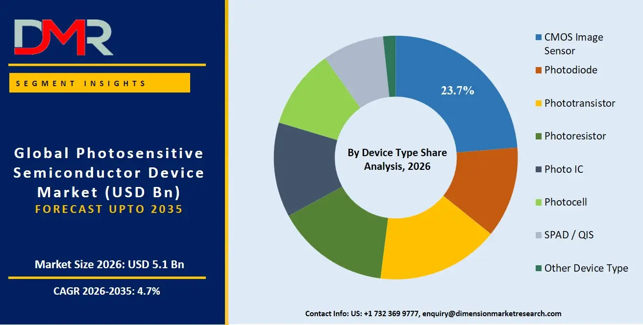
CMOS image sensors is projected to command the largest share of the market due to their combination of low power consumption, compactness, rapid readout speeds, and high levels of on-chip integration. These advantages make them indispensable in smartphones, digital cameras, advanced driver-assistance systems, security equipment, and industrial automation. Ongoing technological progress, including backside-illuminated structures, stacked sensor designs, and improved pixel architectures, continues to enhance sensitivity, dynamic range, and image quality. Their compatibility with cost-efficient semiconductor manufacturing processes further supports widespread adoption. As demand for high-resolution imaging and intelligent vision systems grows across both consumer and industrial sectors, CMOS image sensors are expected to maintain their leadership position and remain the cornerstone of photosensitive semiconductor technology.
By Material Analysis
Silicon is poised to remain the dominant material in photosensitive semiconductor devices because it offers an exceptional balance of performance, availability, and affordability. Decades of investment in silicon fabrication infrastructure have created a highly efficient supply chain and a mature manufacturing ecosystem capable of producing devices at enormous scale. Silicon's favorable electronic and optical properties enable reliable operation in photodiodes, image sensors, and related components used in diverse applications. In addition, its seamless compatibility with standard CMOS processing facilitates the integration of sensing and signal-processing functions on a single chip, reducing system complexity and cost. These advantages ensure silicon's continued prominence despite the emergence of specialized compound semiconductor materials for niche applications.
By Spectral Response Analysis
Devices optimized for the visible spectrum is expected to account for the largest market share because they support the widest array of end-use applications. Consumer cameras, machine vision systems, surveillance equipment, automotive imaging platforms, and numerous industrial inspection tools all rely primarily on visible-light detection. The pervasive presence of imaging functions in everyday electronic products sustains substantial and recurring demand for these devices. Furthermore, advances in sensor sensitivity, color fidelity, and low-light performance continue to expand their utility and value. Since human vision itself operates in the visible range, technologies designed to capture and process visible light naturally occupy a central role in modern electronics, ensuring enduring market leadership for this segment.
By Operating Mode Analysis
Photovoltaic-mode operation is anticipated to lead the market because it delivers low-noise performance, excellent linearity, and reduced power consumption. In this mode, incident light generates a measurable voltage or current without the need for significant external bias, minimizing dark current and enhancing signal integrity. These characteristics are particularly valuable in precision imaging, optical communication, scientific instrumentation, and measurement systems where accuracy is paramount. The mode also contributes to simpler circuit designs and improved energy efficiency, qualities that are increasingly important in portable and battery-powered devices. As applications continue to demand higher sensitivity and reliability, photovoltaic operation remains the preferred choice for a broad range of photosensitive semiconductor technologies.
By Application Analysis
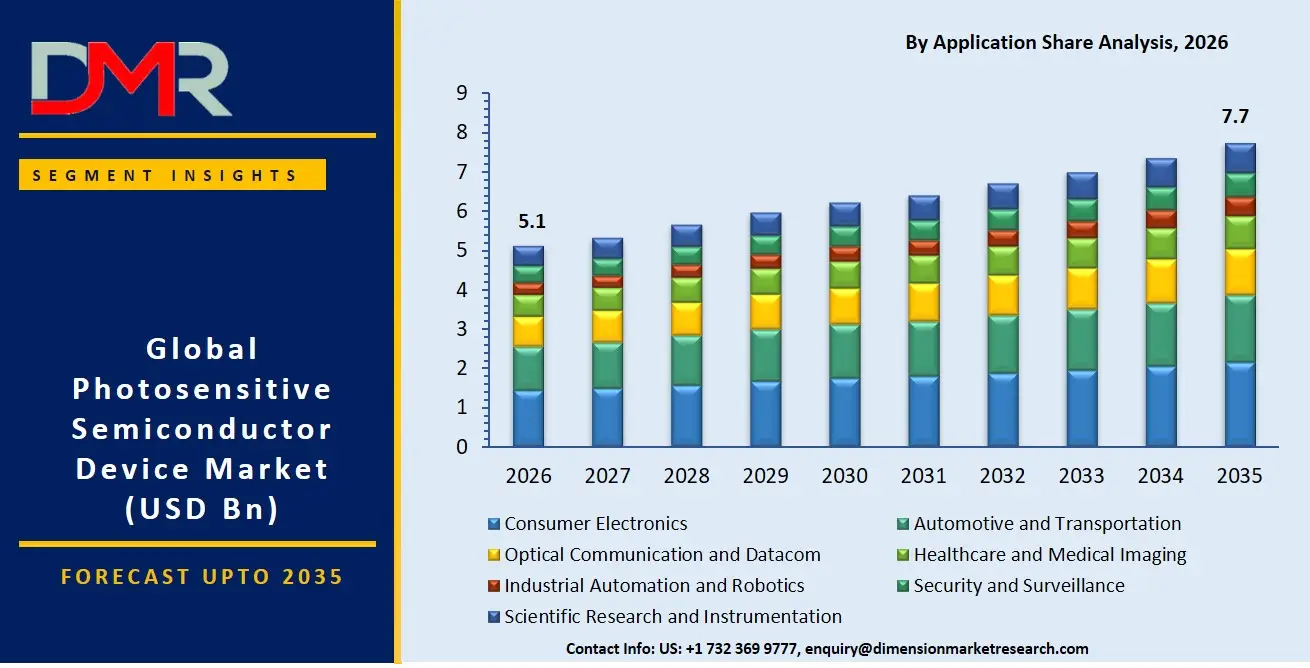
Consumer electronics are expected to constitute the largest application segment, fueled by the enormous production volumes of smartphones, tablets, laptops, wearables, and smart home products. Modern devices increasingly incorporate multiple cameras and optical sensors to enable photography, facial recognition, gesture control, and environmental monitoring.
ℹ
To learn more about this report –
Download Your Free Sample Report Here
Rapid innovation cycles encourage continual upgrades in sensor resolution, speed, and functionality, driving sustained demand for advanced photosensitive semiconductors. The global reach of consumer electronics brands and the widespread adoption of connected devices further reinforce this segment's dominance. As emerging technologies such as augmented reality and intelligent personal devices gain traction, the consumer electronics sector is poised to remain the principal driver of market growth.
By End User Analysis
Consumer electronics original equipment manufacturers are poised to represent the leading end-user group because they integrate vast quantities of image sensors, photodiodes, and related components into mass-market products. Their relentless focus on enhancing user experiences through superior imaging, biometric authentication, and intelligent sensing capabilities generates consistent demand for cutting-edge photosensitive devices. Large production scales allow these manufacturers to rapidly adopt technological advancements and influence industry standards. In addition, frequent product refresh cycles and intense competition encourage continuous investment in sensor innovation. The combination of high shipment volumes, broad product portfolios, and strong emphasis on advanced functionality ensures that consumer electronics OEMs remain the dominant source of demand within the photosensitive semiconductor device market.
The Global Photosensitive Semiconductor Device Market Report is segmented on the basis of the following:
By Device Type
- CMOS Image Sensor
- BSI Sensor
- Stacked Sensor
- Photocell
- Photodiode
- PIN Photodiode
- PN Photodiode
- Avalanche Photodiode
- Schottky Photodiode
- Phototransistor
- Photoresistor
- Photo IC
- SPAD / QIS
- Other Device Type
By Material
- Silicon
- Gallium Arsenide (GaAs)
- Indium Gallium Arsenide (InGaAs)
- Germanium
- Other Semiconductor Materials
By Spectral Response
- Ultraviolet (UV)
- Visible
- Near-Infrared (NIR)
- Infrared (IR)
By Operating Mode
- Photovoltaic Mode
- Photoconductive Mode
- Avalanche Mode
By Application
- Consumer Electronics
- Smartphones and Tablets
- Wearables and AR/VR
- Digital Cameras and Smart Home Devices
- Optical Communication and Datacom
- Fiber-Optic Receivers
- Optical Transceivers
- Data Center Interconnects
- Automotive and Transportation
- LiDAR
- ADAS Cameras
- In-Cabin Monitoring Systems
- Healthcare and Medical Imaging
- X-ray Detectors
- Endoscopy Systems
- Patient Monitoring and Diagnostic Devices
- Industrial Automation and Robotics
- Machine Vision Systems
- Position and Proximity Sensing
- Robotic Guidance and Inspection
- Security and Surveillance
- CCTV Cameras
- Biometric Recognition Systems
- Perimeter Intrusion Detection
- Scientific Research and Instrumentation
- Spectroscopy Equipment
- Astronomical Detectors
- Laboratory Analytical Instruments
By End User
- Consumer Electronics OEMs
- Automotive OEMs
- Aerospace and Defence Contractors
- Healthcare Device Manufacturers
- Industrial and Manufacturing Firms
Regional Analysis
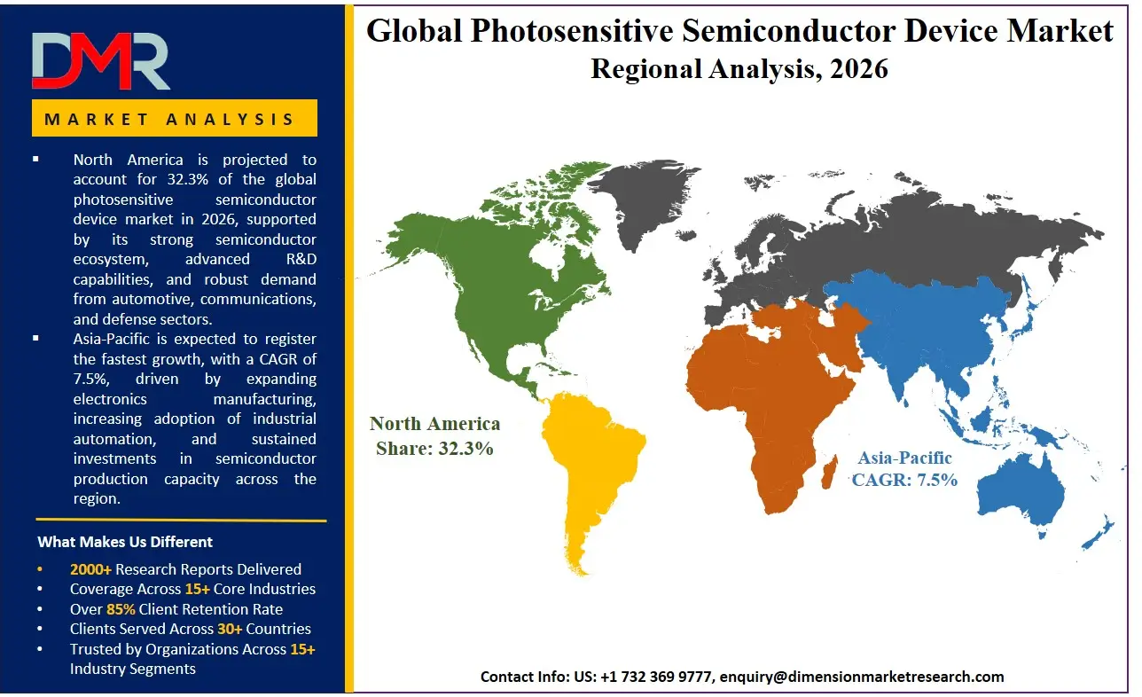
Leading Region by Market Share
ℹ
To learn more about this report –
Download Your Free Sample Report Here
Asia-Pacific (APAC) is poised to dominate the global photosensitive semiconductor device market, commanding a projected 38.1% share by 2026. This leadership is anchored by the region's unassailable position as the global hub for consumer electronics manufacturing, with giants in South Korea, China, and Japan driving colossal demand for CMOS Image Sensors for smartphones and tablets. Furthermore, the rapidly expanding automotive production base, particularly in China and ANZ, is a significant consumer of LiDAR and ADAS camera components. This dense concentration of both supply and demand, supported by massive semiconductor fabrication investments, solidifies APAC's leading position.
Fastest-Growing Regional Market
Asia-Pacific, in addition to being the market leader, is also expected to be the fastest-growing region. The growth is propelled by aggressive national industrial policies focused on electric and autonomous vehicles, as well as the rapid modernization of industrial sectors in China and Southeast Asia. This creates a dual engine of growth: consumer-driven demand for advanced features in smartphones and automotive-driven demand for advanced mobility solutions. The local push to build up domestic semiconductor supply chains for compound materials like GaAs and InGaAs will further reduce costs and accelerate adoption in optical communication and LiDAR, cementing APAC's high-speed growth trajectory.
By Region
North America
Europe
- Germany
- The U.K.
- France
- Italy
- Russia
- Spain
- Benelux
- Nordic
- Rest of Europe
Asia-Pacific
- China
- Japan
- South Korea
- India
- ANZ
- ASEAN
- Rest of Asia-Pacific
Latin America
- Brazil
- Mexico
- Argentina
- Colombia
- Rest of Latin America
Middle East & Africa
- Saudi Arabia
- UAE
- South Africa
- Israel
- Egypt
- Rest of MEA
Competitive Landscape
The competitive landscape of the global photosensitive semiconductor device market is a complex ecosystem where integrated device manufacturers (IDMs), fabless chip companies, and specialized foundries vie for position. Key competitive factors include pixel architecture innovation, proprietary manufacturing processes for 3D stacking and wafer-level bonding, and deep customer relationships with automotive and consumer electronics OEMs. Success hinges on achieving a balance of high-volume manufacturing for smartphones with the high-reliability standards required for automotive and medical applications. Strategic partnerships with LiDAR developers and optical transceiver module makers are critical for gaining design wins in high-growth Optical Communication and Automotive verticals.
Some of the prominent players in the Global Photosensitive Semiconductor Device Market are:
- Hamamatsu Photonics K.K.
- Sony Semiconductor Solutions Corporation
- onsemi
- ams-OSRAM AG
- STMicroelectronics N.V.
- ROHM Co., Ltd.
- Vishay Intertechnology, Inc.
- Broadcom Inc.
- TE Connectivity Ltd.
- OmniVision Technologies, Inc.
- Samsung Electronics Co., Ltd.
- Canon Inc.
- Toshiba Electronic Devices & Storage Corporation
- Sharp Corporation
- Excelitas Technologies Corp.
- First Sensor AG
- Infineon Technologies AG
- Texas Instruments Incorporated
- Panasonic Holdings Corporation
- Renesas Electronics Corporation
- Other Key Players
Recent Developments
- In October 2025, Samsung System LSI introduced the ISOCELL HP7, a 200-megapixel image sensor featuring 0.56-µm pixels and 16-in-1 pixel binning, engineered to deliver sharper detail, improved low-light performance, and enhanced computational photography capabilities for flagship smartphone camera systems.
- In November 2025, ON Semiconductor and Hesai Group publicly agreed to jointly co-develop avalanche photodiode arrays targeting sub-$500 LiDAR units, with pilot production slated for Q2 2026, signaling a direct industry push toward affordable, automotive-grade solid-state LiDAR sensing solutions.
- In June 2025, Sony Semiconductor Solutions officially announced its stacked SPAD depth sensor, the IMX479, for automotive LiDAR applications, delivering high-resolution, high-speed performance and positioning the company to support the industry's continued advancement toward Level 3 autonomous driving capabilities.
Report Details
| Report Characteristics |
| Market Size (2026) |
USD 5.1 Bn |
| Forecast Value (2035) |
USD 7.7 Bn |
| CAGR (2026–2035) |
4.7% |
| The US Market Size (2026) |
USD 1.4 Bn |
| Historical Data |
2021 – 2025 |
| Forecast Data |
2027 – 2035 |
| Base Year |
2025 |
| Estimate Year |
2026 |
| Segments Covered |
By Device Type, By Material, By Spectral Response, By Operating Mode, By Application, and By End User |
| Regional Coverage |
North America – The US and Canada; Europe – Germany, The UK, France, Russia, Spain, Italy, Benelux, Nordic, & Rest of Europe; Asia-Pacific – China, Japan, South Korea, India, ANZ, ASEAN, Rest of APAC; Latin America – Brazil, Mexico, Argentina, Colombia, Rest of Latin America; Middle East & Africa – Saudi Arabia, UAE, South Africa, Turkey, Egypt, Israel, & Rest of MEA |
Frequently Asked Questions
How big is the Photosensitive Semiconductor Device Market?
▾ The Global Photosensitive Semiconductor Device Market is valued at USD 5.1 billion in 2026 and is projected to reach USD 7.7 billion by 2035, fueled by expanding sensing applications across automotive, consumer electronics, and optical communication sectors.
What is the CAGR of the Photosensitive Semiconductor Device Market from 2026 to 2035?
▾ The market is expected to grow at a steady CAGR of 4.7% from 2026 to 2035, reflecting sustained demand for advanced imaging, LiDAR, and high-speed data communication components across diverse industrial and consumer applications globally.
What factors are driving the growth of the Photosensitive Semiconductor Device Market?
▾ Key drivers include the proliferation of ADAS and autonomous vehicle sensors, expanding hyperscale data center optical interconnects, and relentless smartphone camera innovation, all demanding higher resolution, faster response times, and greater spectral sensitivity.
What are the major trends in the Photosensitive Semiconductor Device Market?
▾ Major trends include the rise of event-based neuromorphic vision sensing, integration of on-sensor AI processing within Photo ICs, rapid advancement of SPAD/QIS arrays for 3D sensing, and growing adoption of NIR/IR spectral response devices.
Which region held the largest share of the Photosensitive Semiconductor Device Market in 2026?
▾ Asia-Pacific commands the largest market share at 38.1% in 2026, driven by its dominant consumer electronics manufacturing base and rapidly expanding automotive production, particularly in China, South Korea, and Japan.
Which region is expected to grow the fastest in the Photosensitive Semiconductor Device Market?
▾ Asia-Pacific is also the fastest-growing region, propelled by aggressive national policies supporting autonomous vehicles, rapid industrial modernization, and local semiconductor supply chain development for compound materials like GaAs and InGaAs.
Who are the key players in the Photosensitive Semiconductor Device Market?
▾ Key players include major IDMs like Sony Semiconductor Solutions, Samsung Electronics, and STMicroelectronics, alongside leading foundries like TSMC and specialized fabless firms focusing on advanced CMOS, SPAD, and InGaAs photodiode technologies.
How is the Photosensitive Semiconductor Device Market segmented?
▾ The market is segmented by Device Type, Material, Spectral Response, Operating Mode, Application, and End User, covering diverse components from CMOS Image Sensors to SPADs and photodiodes.