Market Overview
The Global Semiconductor Wafer Market size is projected to reach USD 24.0 billion in 2025 and grow at a compound annual growth rate of 5.9% to reach a value of USD 40.2 billion in 2034.
A semiconductor wafer, often referred to as a substrate, is a thin slice of semiconductor material commonly silicon—that serves as the foundational platform for fabricating integrated circuits (ICs), microchips, and other microelectronic devices. These wafers undergo a series of complex processes, including doping, etching, deposition, and photolithography to create the circuitry that powers everything from smartphones to supercomputers. As the demand for smaller, faster, and more energy-efficient electronics grows, semiconductor wafers have become critical to innovation in digital technology.

The global semiconductor wafer market plays a vital role across various industries such as consumer electronics, automotive, telecommunications, healthcare, and industrial automation. These sectors rely heavily on advanced chips for everything from data processing to connectivity and energy management. In particular, automotive applications like electric vehicles (EVs) and advanced driver-assistance systems (ADAS) are pushing demand for more durable and efficient wafers that can handle higher voltages and temperatures.
One of the most important technological shifts in the industry is the transition to larger wafer sizes—from 200mm to 300mm, and increasingly toward 450mm. Larger wafers allow for more chips to be produced per batch, improving yield and reducing manufacturing costs. This scale-up is crucial to meeting the rising global demand for semiconductors, especially in high-volume applications like smartphones and cloud computing infrastructure. Additionally, the adoption of advanced wafer types like Silicon-On-Insulator (SOI) and compound materials such as Gallium Nitride (GaN) and Silicon Carbide (SiC) is expanding due to their superior performance in power and high-frequency applications.

The market’s growth is further supported by regional manufacturing expansions and government incentives, particularly in the U.S., Europe, and Asia. Initiatives like the CHIPS Act in the U.S. and EU Chips Act in Europe are accelerating domestic wafer production, strengthening supply chains, and encouraging technological innovation.
The US Semiconductor Wafer Market
The US Semiconductor Wafer Market size is projected to reach USD 5.0 billion in 2025 at a compound annual growth rate of 5.5% over its forecast period.
The US holds a dominant position in the semiconductor wafer market due to its robust ecosystem of design, fabrication, and advanced packaging. Key players such as Intel and GlobalFoundries, alongside fabless giants like NVIDIA and Qualcomm, are driving innovation. Government initiatives like the CHIPS Act have injected billions into domestic manufacturing and R&D. In 2025, the US is experiencing a boom in wafer fab construction, particularly in Arizona and Texas. Demand from AI, defense, and EV sectors is further boosting local wafer production and new material development, including GaN and SiC.

Europe Semiconductor Wafer Market
Europe Semiconductor Wafer Market size is projected to reach USD 5.1 billion in 2025 at a compound annual growth rate of 5.2% over its forecast period.
Europe’s semiconductor wafer market is expanding steadily, backed by strategic autonomy goals and massive public-private investments. The region’s focus lies in automotive semiconductors, with Germany, France, and the Netherlands being key hubs. The EU Chips Act has allocated billions to strengthen local manufacturing, and leading firms such as Infineon and STMicroelectronics are increasing their wafer capacity. Europe is also becoming a center for innovation in SiC wafers for EVs and renewables, reflecting its climate goals and industrial strengths.
Japan Semiconductor Wafer Market
Japan Semiconductor Wafer Market size is projected to reach USD 2.9 billion in 2025 at a compound annual growth rate of 5.2% over its forecast period.
Japan remains a critical contributor to the global semiconductor wafer market, thanks to its technological legacy, strong materials industry, and skilled labor force. Major Japanese players like Shin-Etsu Chemical and SUMCO dominate the global supply of silicon wafers. Japan is focusing on expanding domestic chip manufacturing with support from the government, especially in partnership with companies like TSMC. The market is also shifting towards advanced materials like GaN and SiC, used heavily in EVs, power electronics, and communication infrastructure.
Semiconductor Wafer Market: Key Takeaways
- Market Growth: The Semiconductor Wafer Market size is expected to grow by USD 15.0 billion, at a CAGR of 5.9%, during the forecasted period of 2026 to 2034.
- By Wafer Size: The 300 mm segment is anticipated to get the majority share of the Semiconductor Wafer Market in 2025.
- By Application: The consumer electronics segment is expected to get the largest revenue share in 2025 in the Semiconductor Wafer Market.
- Regional Insight: Asia Pacific is expected to hold a 55.0% share of revenue in the Global Semiconductor Wafer Market in 2025.
- Use Cases: Some of the use cases of Semiconductor Wafer include automotive, industrial, and more.
Semiconductor Wafer Market: Use Cases
- Consumer Electronics: Used in smartphones, tablets, and laptops to build compact, high-speed integrated circuits.
- Automotive: Enable ADAS, power management, and battery control systems in electric and autonomous vehicles.
- Industrial: Essential for industrial IoT, sensors, automation, and robotics requiring durable, high-performance chips.
- Telecommunications: Power the backbone of 5G networks and high-frequency RF applications.
Stats & Facts
- The European Commission has committed over EUR 43 billion in public and private funding to boost semiconductor manufacturing by 2030.
- METI (Japan) reports that Japan supplies over 50% of the world’s 300mm silicon wafers.
- According to SEMI, global wafer shipments are expected to reach a new record high in 2025, driven by automotive and AI demand.
Market Dynamic
Driving Factors in the Semiconductor Wafer Market
Technological Advancements and Demand for High-Performance Devices
The growing complexity of applications in AI, cloud computing, and edge devices requires faster and more efficient chips. This is pushing manufacturers to adopt larger wafers (300mm and 450mm) and advanced materials like GaN and SiC to meet power and thermal efficiency needs. As semiconductor nodes shrink and functionalities increase, wafer technology is evolving rapidly to keep pace.
Government Support and Strategic Investments
Governments across the globe are recognizing the strategic importance of semiconductor manufacturing. Incentives, subsidies, and national policies—like the US CHIPS Act, the EU Chips Act, and Japan’s tech funds—are injecting billions into domestic wafer production facilities. These initiatives are creating favorable conditions for both existing and new players to invest in cutting-edge wafer fabs.
Restraints in the Semiconductor Wafer Market
High Cost of Advanced Wafer Fabrication
Building and maintaining state-of-the-art wafer fabs involves significant capital expenditure, often running into billions of dollars. Additionally, the cost of producing advanced wafers using newer materials or larger sizes can be prohibitively high, especially for small to mid-sized companies, creating a high entry barrier in the market.
Global Supply Chain Vulnerabilities
The semiconductor wafer market remains highly sensitive to geopolitical tensions, trade restrictions, and raw material shortages. Disruptions caused by events like the COVID-19 pandemic or export controls on key materials have exposed the fragility of global supply chains, leading to production delays and cost spikes for manufacturers.
Opportunities in the Semiconductor Wafer Market
Rise of Electric Vehicles and Smart Mobility
The global transition toward EVs is creating a huge opportunity for semiconductor wafers, particularly those made of SiC and GaN, which are ideal for high-power and high-temperature applications. Increased use of power electronics in EV drivetrains and charging infrastructure is driving demand for durable, high-efficiency wafers.
Expansion of IoT and Edge Computing
The growing deployment of IoT devices across homes, factories, and cities is fueling demand for smaller, power-efficient semiconductor chips. This, in turn, increases the demand for specialty wafers that support low-power nodes and embedded systems. Wafers tailored for edge computing devices are expected to gain traction, especially in smart industrial and healthcare applications.
Trends in the Semiconductor Wafer Market
Adoption of Compound Semiconductors
Materials like Gallium Nitride (GaN) and Silicon Carbide (SiC) are becoming mainstream, especially for applications requiring high voltage and thermal performance. These compound semiconductor wafers are gaining popularity in sectors like EVs, renewables, and aerospace, where traditional silicon-based wafers fall short.
Shift to 450mm Wafers for Mass Production
Though still in its early phases, the move toward 450mm wafers is gaining attention due to their potential to significantly improve productivity and reduce costs. Industry leaders are experimenting with pilot lines, and large-scale adoption may transform the economics of chip manufacturing in the coming years.
Impact of Artificial Intelligence in Semiconductor Wafer Market
- AI-Driven Wafer Inspection: Machine learning enhances wafer defect detection, reducing waste and improving quality control in fabs.
- Smart Yield Optimization: AI models help in real-time process adjustments, maximizing wafer yield and reducing costs.
- Predictive Maintenance: AI monitors fab equipment, predicting potential failures to avoid downtime and maintain consistent wafer output.
- Faster R&D Cycles: AI accelerates material discovery and simulation for new wafer types, reducing time-to-market.
- Design Automation: AI improves chip design tools, allowing better wafer utilization and performance optimization.
Research Scope and Analysis
By Wafer Size Analysis
300 mm wafers are expected to dominate the semiconductor wafer market in 2025, accounting for nearly 50% of the global share. These wafers offer a superior cost-to-output ratio and are widely used in high-volume production for consumer electronics, computing devices, and telecom infrastructure. Their ability to support advanced process nodes (such as 7nm, 5nm, and below) makes them ideal for modern chip designs.
Major manufacturers have heavily invested in 300 mm wafer fabs to meet growing demand across AI, 5G, and cloud computing sectors. Their extensive deployment across applications and mature supply chain ecosystem contribute significantly to their leading position in the market. Additionally, equipment manufacturers have developed robust systems tailored for 300 mm wafers, further solidifying their scalability and economic feasibility in global chip production.
450 mm wafers are emerging as the fastest-growing wafer size segment, despite still being in early adoption phases. Their appeal lies in their significantly larger surface area, which allows for more chips per wafer—substantially reducing production costs at scale. Though commercial deployment is limited, pilot fabs in Asia and the U.S. are exploring 450 mm wafer production for high-performance computing and AI-based applications.
These wafers can enhance manufacturing throughput, cut down per-chip costs, and optimize fab operations once the required tooling and infrastructure are in place. The growth in demand for powerful chips—especially in data centers and supercomputing—creates the necessary incentive to shift toward 450 mm wafers. Their long-term economic potential and ability to meet growing performance demands position them as a transformative force in future semiconductor manufacturing.
By Wafer Type Analysis
Polished wafers hold the largest market share in 2025, being the foundational substrate for integrated circuit manufacturing. These wafers undergo chemical and mechanical polishing to provide the ultra-smooth, defect-free surfaces required for photolithography and etching processes in semiconductor fabrication. Used in nearly every electronic device, from smartphones and laptops to automotive microcontrollers, polished wafers remain indispensable across the value chain.
Their consistent thickness and high flatness contribute to the high yield and performance of devices built upon them. As chip designs become more compact and complex, the need for uniform, high-quality polished wafers continues to rise. With their broad utility, established manufacturing processes, and compatibility across legacy and cutting-edge nodes, polished wafers will maintain their leading position, particularly in consumer electronics and general-purpose IC production.
Further, Silicon-On-Insulator (SOI) wafers are the fastest-growing wafer type, seeing accelerating adoption in RF, automotive, and low-power applications. SOI wafers consist of a thin silicon layer separated from the bulk substrate by an insulating oxide layer, which significantly reduces parasitic capacitance and improves performance. This structure enhances power efficiency and switching speed—critical for 5G RF chips, automotive safety systems, and battery-operated devices.
Demand is especially high in smartphones for RF front-end modules, and in automotive electronics requiring energy-efficient and thermally stable components. Additionally, their integration into advanced logic and photonics platforms is gaining momentum. SOI wafer growth is supported by expanding production capabilities from suppliers like Soitec and increasing design activity from OEMs prioritizing performance-per-watt optimization.
By Material Analysis
Silicon continues to dominate the semiconductor wafer market, expected to hold more than 60% share in 2025. As the most widely used and cost-effective semiconductor material, silicon benefits from decades of manufacturing maturity, a vast supply chain, and extensive equipment compatibility. It is well-suited for mainstream electronics, including logic ICs, memory, and analog devices.
Foundries and IDMs have optimized fabrication processes around silicon, enabling high yields and device reliability at shrinking process nodes. Its properties allow for precise doping, etching, and layer deposition, making it ideal for producing transistors and other integrated components. Silicon’s scalability and affordability ensure its continued use across industries, particularly in consumer electronics and computing, where performance demands align with its capabilities.
Silicon Carbide (SiC) stands out as the fastest-growing wafer material segment due to its suitability for high-voltage, high-temperature, and high-efficiency applications. Unlike silicon, SiC has a wider bandgap, higher thermal conductivity, and can operate at elevated temperatures, making it perfect for electric vehicles, industrial motor drives, and renewable energy inverters.
As global EV adoption accelerates, automotive manufacturers are increasingly turning to SiC-based power devices to improve drivetrain efficiency and extend battery range. Additionally, SiC’s role in enabling compact and efficient power electronics makes it vital in high-demand sectors like aerospace and smart grids. With the increasing number of 800V EV architectures and SiC production expansion by players like Wolfspeed and STMicroelectronics, this material is poised for explosive growth over the coming years.
By Application Analysis
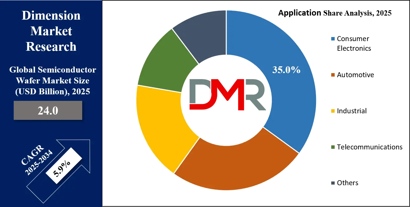
Consumer electronics remain the dominant application for semiconductor wafers in 2025, holding the largest share of 35% due to the massive and consistent demand for smartphones, laptops, tablets, and wearable devices. These devices require a broad range of semiconductor chips—from microprocessors and memory to sensors and power management ICs—all fabricated on high-purity silicon wafers.
The miniaturization of consumer electronics is driving demand for advanced node chips, increasing the use of 300 mm wafers for high-volume production. The rise in AI features in mobile devices, including image processing, voice recognition, and AR applications, also boosts wafer consumption. The consumer electronics industry’s fast product cycles, high unit volumes, and demand for compact, efficient, and reliable chips ensure the continued dominance of this segment.
Automotive is the fastest-growing application segment, driven by the electrification of vehicles, rising use of ADAS, and the growing need for in-vehicle connectivity. Modern vehicles require hundreds of semiconductors for various functions, including powertrain control, infotainment, safety, and navigation.
The shift to electric vehicles (EVs) is particularly accelerating demand for high-performance power semiconductors built on SiC wafers. Additionally, autonomous driving technologies require advanced logic, sensing, and decision-making hardware, increasing the number and complexity of chips per vehicle. Government regulations promoting EVs and safety mandates are pushing automakers to adopt next-gen semiconductor solutions, making automotive the most dynamic and rapidly expanding application for wafer manufacturers in the current decade.
By End User Analysis
Integrated Device Manufacturers (IDMs) are expected to lead the end-user segment in 2025, accounting for the largest share of the global semiconductor wafer market. IDMs such as Intel, Samsung, and Texas Instruments manage the entire value chain—from chip design to wafer fabrication and packaging—enabling full control over quality, costs, and innovation.
This vertical integration allows them to develop custom process technologies, optimize manufacturing for specific products, and secure supply in a volatile market. IDMs benefit from economies of scale, deep R&D capabilities, and access to long-term contracts with major electronics and automotive customers. Their investments in next-generation wafer fabs, particularly for AI, high-performance computing, and automotive applications, ensure their continued dominance across multiple wafer types and materials.
Foundries represent the fastest-growing end-user segment, fueled by the expansion of fabless semiconductor companies worldwide. Foundries such as TSMC, GlobalFoundries, and UMC specialize in contract wafer manufacturing for clients who design chips but lack fabrication capacity. The rising complexity and cost of semiconductor manufacturing have made the fabless-foundry model highly attractive, especially for startups and mid-sized firms focused on innovation.
Foundries are scaling up capacity, offering advanced process nodes, and diversifying material support—including SiC and SOI wafers—to meet varied client needs. Their flexible manufacturing services and partnerships with key technology companies make them indispensable in today’s fast-evolving semiconductor ecosystem, particularly in AI, automotive, and consumer markets.
The Semiconductor Wafer Market Report is segmented on the basis of the following:
By Wafer Size
- 150 mm
- 200 mm
- 300 mm
- 450 mm
By Wafer Type
- Polished Wafer
- Epitaxial Wafer
- SOI (Silicon-On-Insulator) Wafer
- Diffusion Wafer
By Material
- Silicon
- GaAs (Gallium Arsenide)
- SiC (Silicon Carbide)
- GaN (Gallium Nitride)
- Others
By Application
- Consumer Electronics
- Automotive
- Industrial
- Telecommunications
- Others
By End User
- Foundries
- IDMs (Integrated Device Manufacturers)
- OSATs (Outsourced Semiconductor Assembly and Test)
Regional Analysis
Leading Region in the Semiconductor Wafer Market
Asia Pacific dominates the global semiconductor wafer market, with a projected share of 55% in 2025, owing to its established manufacturing ecosystem, abundant skilled labor, and presence of global wafer suppliers and foundries. Countries like Taiwan, South Korea, China, and Japan serve as major hubs for wafer production and innovation. Taiwan's TSMC, South Korea’s Samsung, and Japan’s SUMCO and Shin-Etsu Chemical are global leaders in wafer fabrication and material supply. These nations benefit from a robust supply chain, proximity to consumer electronics manufacturing, and strong government support through incentives and R&D funding.
Additionally, regional governments are aggressively investing in semiconductor self-reliance and expansion of fab capacities to meet domestic and global demand. The rise of electric vehicles, 5G, and industrial automation in Asia further boosts local wafer consumption. With continuous investment in advanced process nodes, larger wafer sizes, and compound materials, Asia Pacific is expected to maintain its leadership in both volume and innovation.

Fastest Growing Region in the Semiconductor Wafer Market
North America, led by the United States, is the fastest-growing region in the semiconductor wafer market in 2025, propelled by significant federal and private investments aimed at revitalizing domestic chip manufacturing. The CHIPS and Science Act has allocated over USD 50 billion to strengthen the U.S. semiconductor supply chain, including wafer production and material sourcing. Companies like Intel, GlobalFoundries, TSMC, and Micron are building or expanding fabrication facilities in states like Arizona, Texas, and New York.
This surge is driven by the need for strategic independence, especially in light of global supply disruptions and geopolitical tensions. North America's growing demand for advanced semiconductor applications in AI, defense, automotive, and high-performance computing is also catalyzing wafer production growth. Moreover, increased R&D funding is fostering innovation in new wafer materials like SiC and GaN, positioning the region not just as a consumer but also as a key production hub for next-generation semiconductors.
By Region
North America
Europe
- Germany
- The U.K.
- France
- Italy
- Russia
- Spain
- Benelux
- Nordic
- Rest of Europe
Asia-Pacific
- China
- Japan
- South Korea
- India
- ANZ
- ASEAN
- Rest of Asia-Pacific
Latin America
- Brazil
- Mexico
- Argentina
- Colombia
- Rest of Latin America
Middle East & Africa
- Saudi Arabia
- UAE
- South Africa
- Israel
- Egypt
- Rest of MEA
Competitive Landscape
The semiconductor wafer market is moderately consolidated, with major players including TSMC, Samsung Electronics, GlobalFoundries, SUMCO Corporation, Siltronic AG, Shin-Etsu Chemical Co., Ltd., and Intel Corporation. These companies dominate due to advanced wafer processing capabilities, large-scale manufacturing, and global reach. Strategies such as geographic expansion, R&D investments, partnerships with automotive and AI companies, and vertical integration are common. The rise of specialized wafer types like SOI, SiC, and GaN is creating opportunities for niche players and material innovators. Meanwhile, regional investments in the U.S., Japan, and Europe are intensifying competition and fostering the development of localized supply chains.
Some of the prominent players in the global Semiconductor Wafer are:
- Micron
- TSMC
- SUMCO Corporation
- GlobalFoundries
- STMicroelectronics
- Siltronic AG
- SK Siltron Co., Ltd.
- Soitec S.A.
- Okmetic Oyj
- Wafer Works Corporation
- National Silicon Industry Group (NSIG)
- Zhejiang Jingsheng Mechanical & Electrical Co., Ltd.
- Hangzhou Silan Microelectronics Co., Ltd.
- Shanghai Simgui Technology Co., Ltd.
- Topsil Semiconductor Materials A/S
- MEMC Electronic Materials, Inc. (SunEdison Semiconductor)
- Ferrotec Holdings Corporation
- Episil-Precision Inc.
- Advanced Silicon Group
- Hangzhou Haina Semiconductor Co., Ltd.
- Zhonghuan Semiconductor Co., Ltd. (TCL Zhonghuan)
- GRITEK Semiconductor Co., Ltd.
- Other Key Players
Recent Developments
- In May 2025, GlobalFoundries acquired a MEMS wafer facility in New York, boosting its capabilities in specialty wafers for automotive sensors and IoT.
- In April 2025, STMicroelectronics and Soitec partnered to scale up SOI wafer production in Europe, supporting RF and low-power applications.
- In February 2025, TSMC opened its first fab in Kumamoto, Japan, in partnership with Sony and Denso, producing 22/28nm wafers for automotive semiconductors.
Report Details
| Report Characteristics |
| Market Size (2025) |
USD 24.0 Bn |
| Forecast Value (2034) |
USD 40.2 Bn |
| CAGR (2025–2034) |
5.9% |
| The US Market Size (2025) |
USD 5.0 Bn |
| Historical Data |
2019 – 2024 |
| Forecast Data |
2026 – 2034 |
| Base Year |
2024 |
| Estimate Year |
2025 |
| Report Coverage |
Market Revenue Estimation, Market Dynamics, Competitive Landscape, Growth Factors, etc. |
| Segments Covered |
By Wafer Size (150 mm, 200 mm, 300 mm, and 450 mm), By Wafer Type (Polished Wafer, Epitaxial Wafer, SOI (Silicon-On-Insulator) Wafer, and Diffusion Wafer), By Material (Silicon, GaAs (Gallium Arsenide), SiC (Silicon Carbide), GaN (Gallium Nitride), and Others), By Application (Consumer Electronics, Automotive, Industrial, Telecommunications, and Others), By End User (Foundries, IDMs (Integrated Device Manufacturers), and OSATs (Outsourced Semiconductor Assembly and Test)) |
| Regional Coverage |
North America – US, Canada; Europe – Germany, UK, France, Russia, Spain, Italy, Benelux, Nordic, Rest of Europe; Asia-Pacific – China, Japan, South Korea, India, ANZ, ASEAN, Rest of APAC; Latin America – Brazil, Mexico, Argentina, Colombia, Rest of Latin America; Middle East & Africa – Saudi Arabia, UAE, South Africa, Turkey, Egypt, Israel, Rest of MEA |
| Prominent Players |
Micron, TSMC, SUMCO Corporation, GlobalFoundries, STMicroelectronics, Siltronic AG, SK Siltron Co., Ltd., Soitec S.A., Okmetic Oyj, Wafer Works Corporation, National Silicon Industry Group (NSIG), Zhejiang Jingsheng Mechanical & Electrical Co., Ltd., Hangzhou Silan Microelectronics Co., Ltd., Shanghai Simgui Technology Co., Ltd., Topsil Semiconductor Materials A/S, MEMC Electronic Materials, Inc. (SunEdison Semiconductor), Ferrotec Holdings Corporation, Episil-Precision Inc., Advanced Silicon Group, Hangzhou Haina Semiconductor Co., Ltd., Zhonghuan Semiconductor Co., Ltd. (TCL Zhonghuan), GRITEK Semiconductor Co., Ltd., and Other Key Players |
| Purchase Options |
We have three licenses to opt for: Single User License (Limited to 1 user), Multi-User License (Up to 5 Users), and Corporate Use License (Unlimited User) along with free report customization equivalent to 0 analyst working days, 3 analysts working days, and 5 analysts working days respectively. |
Frequently Asked Questions
The Global Semiconductor Wafer Market size is expected to reach a value of USD 24.0 billion in 2025 and is expected to reach USD 40.2 billion by the end of 2034.
Asia Pacific is expected to have the largest market share in the Global Semiconductor Wafer Market, with a share of about 55.0% in 2025.
The Semiconductor Wafer Market in the US is expected to reach USD 5.0 billion in 2025.
Some of the major key players in the Global Semiconductor Wafer Market are TSMC, Intel, GlobalFoundries and others
The market is growing at a CAGR of 5.9 percent over the forecasted period.