Market Overview
The surface roughness measurement market covers instruments and software that quantify texture, waviness, and geometric deviation on machined and finished parts. It excludes general dimensional coordinate measuring machines that do not report roughness parameters such as Ra, Rz, or Rq. Quality teams in automotive, semiconductor, and aerospace plants buy these tools to verify that a finished surface meets a defined tolerance before the part ships.
Wafer fabrication plants tightened surface tolerance budgets to sub-nanometer levels as chip nodes shrank, pushing metrology vendors to redesign optical heads for finer resolution. Mahr responded to this shift in July 2024 by acquiring OptoSurf GmbH, adding scattered-light optical metrology and tribological analysis to its product line. Buyers now expect a single vendor to cover both texture and contour measurement rather than sourcing separate instruments for each task.
Machine builders are also folding roughness sensors directly into CNC and grinding lines. This shift moves quality checks from a separate lab station to the production line itself, cutting the time between a bad cut and a corrective adjustment.
Market Size and Forecast
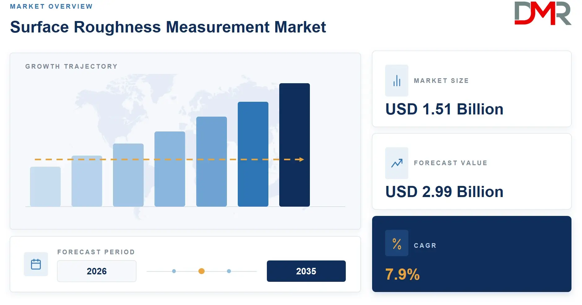
The Global Surface Roughness Measurement Market size is estimated at USD 1.51 Billion in 2026 from USD 1.4 Billion in 2025, and is projected to reach USD 2.99 Billion by 2035, exhibiting a CAGR of 7.9% during the forecast period.
Demand grew steadily through the early 2020s as automotive machine shops standardized roughness checks on CNC lines to cut warranty claims tied to friction and wear. Semiconductor fabs added a second demand layer once node shrinkage forced tighter wafer and MEMS process control. A March 2026 study in Scientific Reports found that a stacking hybrid machine learning model predicted CNC turning surface roughness with an R² of 0.9603 under new tool conditions, a result that supports vendor claims that predictive software can now sit alongside physical measurement hardware.
ℹ
To learn more about this report –
Download Your Free Sample Report Here
Forecast assumptions rest on continued electronics manufacturing expansion in Asia Pacific and on aerospace and medical device programs that require documented topography verification for critical components. Mitutoyo added to this base in January 2025 with the SJ-220 portable tester, built for ISO 21920 compliance and wireless shop-floor use, a sign that portable field instruments will keep gaining share alongside lab-grade optical systems.
Market Snapshot
- Global market size stands at USD 1.4 Billion in 2025.
- The market will reach USD 2.99 Billion by 2035 at a CAGR of 7.9%.
- North America leads with a 36.8% share in 2025.
- Non-Contact techniques dominate with a 64.5% share.
- Optical Profilometry leads the method category with a 37.6% share.
- Automotive holds the top vertical position with a 34.8% share.
- Asia Pacific is the fastest growing region for inline metrology deployment.
Technique Analysis
Non-Contact techniques led the technique segment with a 64.5% share in 2026.
Laser and interferometric heads scan a part without touching it, so plants running high-volume lines prefer this method to avoid stylus wear and part damage. Coherence scanning white-light interferometry now reaches vertical resolution below 1 nm in monochromatic mode on flat samples, a precision level that stylus contact systems cannot match on delicate wafers or optics. Vendors are pricing non-contact heads as the default choice for any line that inspects thousands of parts a day.
Contact stylus systems still hold a role on shop floors that need a rugged, low-cost instrument for spot checks. Machine shops with tight capital budgets often start with a portable stylus tester before upgrading to optical systems once volume justifies the cost. The market is migrating from stylus toward optical and laser methods, but the shift is gradual rather than a full replacement, since many small shops cannot justify the price gap yet.
Method Analysis
With a 37.6% share in 2026, Optical Profilometry outpaced all other method categories.
Optical profilometers capture wide fields of view fast, and Polytec's macro optical system can stitch a scan area from 44 by 33 millimeters up to 230 by 220 millimeters while collecting up to 2 million data points within seconds. That throughput lets a single station cover parts that once needed several stylus passes, cutting inspection time on large aerospace and automotive components.
Stylus profilometry, confocal profilometry, focus variation, X-ray reflectometry, atomic force microscopy, and scanning electron microscopy fill specialized niches. Confocal and focus variation systems serve micro-scale parts where optical profilometers lose accuracy on steep sidewalls. X-ray reflectometry and atomic force microscopy stay confined to semiconductor labs that need sub-nanometer film and surface data. Buyers choosing among these methods weigh sample size, surface reflectivity, and required resolution rather than price alone.
Surface Type Analysis
2D measurement accounted for the dominant share of surface type demand in 2026.
Line-profile 2D measurement remains the default for parts where a single cross-section proves compliance, such as a bearing race or a shaft. Quality managers favor 2D checks because they run fast and match decades of established ISO and ANSI reference standards, keeping audit trails simple.
3D surface measurement is the fastest growing category, driven by parts with complex freeform geometry such as turbine blades and optical lenses. A full-area 3D map catches defects that a single 2D line would miss entirely, and buyers in aerospace and optics are shifting budgets toward 3D-capable systems even though they cost more per station.
Component Analysis
Probes captured the largest share of the component segment in 2026.
Probes and sensor heads carry the highest per-unit price and the most frequent replacement cycle, since styli wear out and optical heads need periodic recalibration. Instrument makers protect margin by bundling proprietary probes with service contracts rather than selling them as commodity parts.
Software is the fastest growing component as vendors add automated defect classification and cloud-linked reporting to compete on features rather than hardware specs alone. Frame grabbers, lighting equipment, and cameras support the imaging chain for optical systems, while a smaller group of other components covers mounts, calibration standards, and enclosures. Vendors that once sold hardware alone are now pricing software subscriptions separately, turning a one-time hardware sale into recurring revenue.
Vertical Analysis
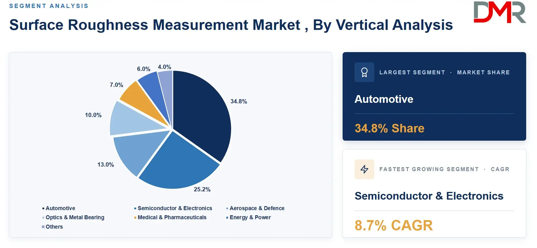
Automotive captured 34.8% of the vertical segment in 2026, ahead of all rivals.
Automotive machine shops standardized Ra, Rz, and Rq inspection on CNC quality lines specifically to cut friction, wear, and warranty-driven defect rates. That standardization created steady, repeat instrument demand across engine, transmission, and bearing production lines rather than a one-time capital purchase.
ℹ
To learn more about this report –
Download Your Free Sample Report Here
Semiconductor and electronics manufacturing is the fastest growing vertical as wafer and MEMS process control tightens alongside node miniaturization. Aerospace and defence, optics and metal bearing, medical and pharmaceuticals, and energy and power round out demand, each buying metrology to satisfy documented compliance standards rather than general quality preference. Vendors that serve automotive at scale are now adapting the same instrument platforms for semiconductor fabs, since both buyers need repeatable, audit-ready data.
Key Market Segments
By Technique
By Method
- Optical Profilometry
- Stylus Profilometry
- Confocal Profilometry
- Focus Variation
- X-ray Reflectometry
- Atomic Force Microscopy (AFM)
- Scanning Electron Microscopy (SEM)
- Others
By Surface Type
By Component
- Probes
- Software
- Frame Grabbers
- Lighting Equipment
- Cameras
- Others
By Vertical
- Automotive
- Semiconductor & Electronics
- Aerospace & Defence
- Optics & Metal Bearing
- Medical & Pharmaceuticals
- Energy & Power
- Others
Regional Analysis
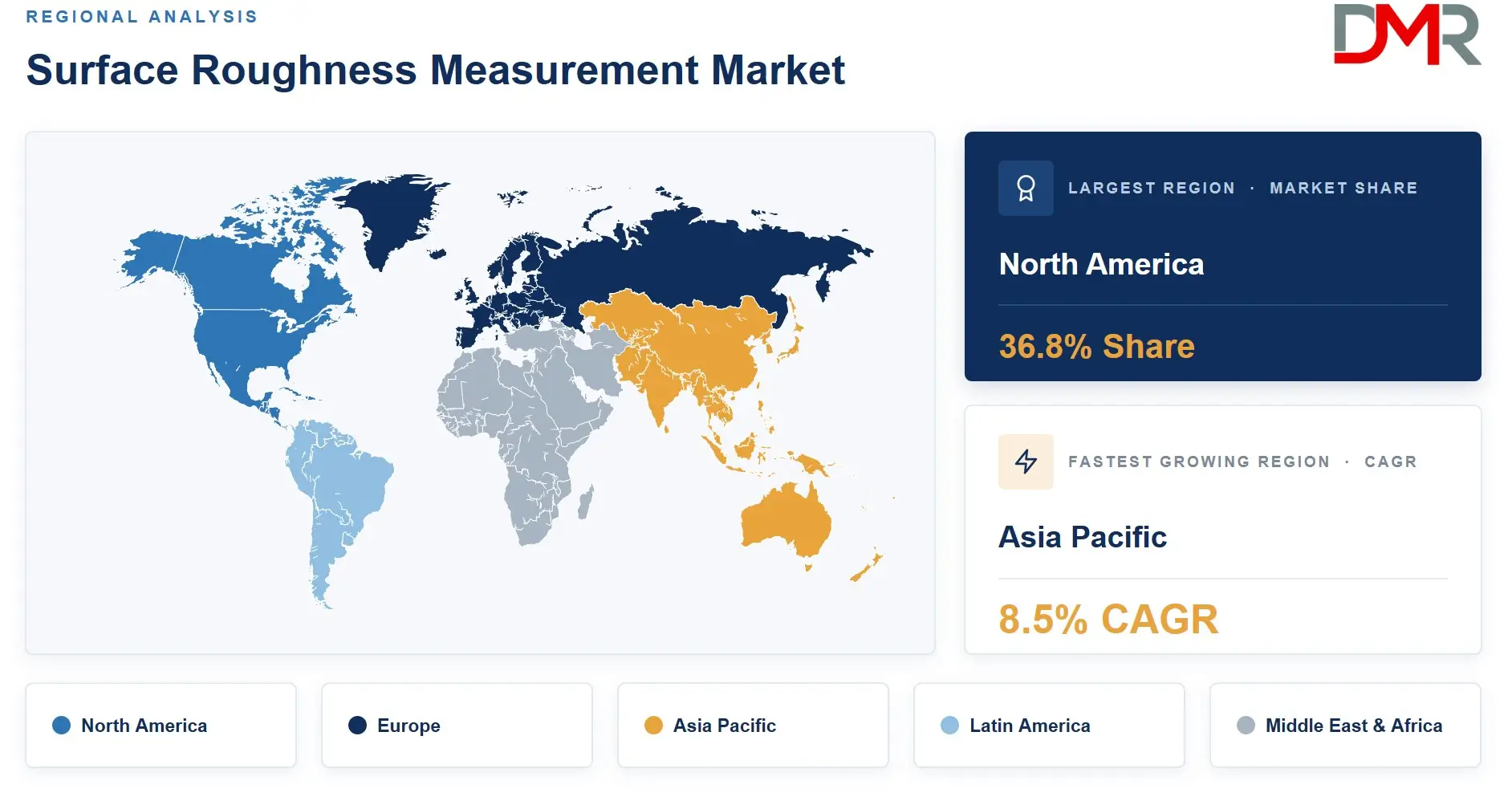
North America led the market with a 36.8% share, worth close to USD 515 Million in 2026.
Established automotive and aerospace manufacturing bases across the US and Canada drive North American demand. Compliance-heavy sectors such as medical device production require documented topography verification on critical components, and plants in the region already run mature quality programs that budget for regular instrument upgrades. The US alone generated USD 302.12 Million in 2025 and is growing at a CAGR of 6.6%.
ℹ
To learn more about this report –
Download Your Free Sample Report Here
Asia Pacific is the fastest growing region, led by electronics and EV component manufacturing hubs in China, South Korea, and India that are expanding inline metrology deployment. Europe holds a steady base built on precision engineering in Germany and instrument manufacturing heritage in Switzerland and the UK. Latin America and Middle East & Africa remain smaller markets today, but growing automotive and energy investment in both regions signals rising instrument demand over the next decade.
Key Regions and Countries
North America
Europe
- Germany
- France
- The UK
- Spain
- Italy
- Rest of Europe
Asia Pacific
- China
- Japan
- South Korea
- India
- Australia
- Rest of APAC
Latin America
- Brazil
- Mexico
- Rest of Latin America
Middle East & Africa
- GCC
- South Africa
- Rest of MEA
Market Dynamics
Chip and Wafer Tolerances Push Metrology Upgrades
Semiconductor fabs shrank node sizes and, in doing so, tightened surface tolerance budgets to sub-nanometer levels for wafer and MEMS process control. Automotive CNC quality lines added a second demand layer by standardizing Ra, Rz, and Rq inspection to cut friction, wear, and warranty-driven defects. Coherence scanning white-light interferometry now supports non-destructive metrology across sample sizes ranging from MEMS chips to full engine blocks.
A June 2025 study on grinding operations found that a tuned support vector regression model predicted surface roughness with an R² of 0.9886 and a mean absolute percentage error under 1%. Fabs and machine shops are pairing physical instruments with this kind of predictive software to catch drift before a part fails inspection, turning metrology into a process control tool rather than a pass or fail gate.
Reflective Surface Limits Cap Optical Adoption
Optical profilometry depends on reflective surfaces, so parts made from dark, rough, or low-reflectivity materials often need coating or preparation before a scan runs cleanly. That extra step adds cost and time, and it discourages shops running high-mix, low-volume production from switching away from stylus systems. Small and mid-volume machine shops also face a real capital barrier, since 3D optical systems carry high upfront cost alongside a need for specialized operator training.
Measurement error compounds the problem. Surface finish instruments carry quality grades with inherent errors ranging from 5% to 25%, driven by vibration, tracing speed, and cutoff wavelength choice. A shop that cannot control its measurement environment risks inconsistent readings regardless of which instrument it buys.
Inline Deployment Opens New Vendor Revenue
Portable stylus instruments are becoming the fastest growing segment by capturing high-volume shop-floor and field inspection work that once required sending parts to a lab. Asia Pacific electronics and EV component hubs represent the largest regional white space, since manufacturing capacity there is expanding faster than installed metrology capacity. Mahr strengthened its position in this space in July 2024 by acquiring OptoSurf GmbH, adding scattered-light optical technology to its roughness and tribology offering.
Inline, production-integrated metrology is replacing offline lab sampling on high-throughput lines, giving plant managers real-time process control instead of delayed batch feedback. Vendors are also bundling roughness and contour measurement into single platforms, consolidating what used to be two separate purchase decisions into one.
Market Trends
Contact Methods Give Way to Optical and Laser Scanning
Buyers are shifting steadily from contact stylus instruments toward non-contact laser and interferometric techniques that inspect without touching or damaging the part. Vendors are also merging roughness texture measurement with contour and geometry inspection into unified machine categories, reshaping how instrument platforms are built. Applications beyond automotive, including solar cells, data storage media, and material science research, are widening the addressable base for these combined platforms.
Market Competition Overview
The market stays fragmented across a long list of specialized instrument makers rather than consolidating around two or three dominant suppliers. Legacy metrology brands hold share through decades of calibration standards recognition and service networks built into automotive and aerospace quality programs. Newer optical and interferometry specialists compete on precision and speed rather than brand history, winning share in semiconductor and electronics accounts where nanometer resolution matters more than an established name.
Consolidation is starting through targeted acquisitions rather than mergers of equals, as larger instrument makers buy specialized optical technology to round out their portfolios instead of building it internally. This pattern favors companies with strong balance sheets and leaves smaller single-technology vendors as likely acquisition targets over the next several years.
Company Profiles
Hexagon AB positions itself as a full-line metrology supplier, pairing surface roughness instruments with its broader coordinate measuring machine and software portfolio. That breadth lets Hexagon sell a single integrated quality system to large automotive and aerospace accounts, reducing the risk that a customer switches to a narrower specialist for one measurement type.
Mitutoyo Corporation built its position on portable, field-ready instruments, reinforced by the January 2025 launch of the SJ-220 tester with wireless connectivity and ISO 21920 compliance. This focus on shop-floor usability gives Mitutoyo an advantage with mid-size manufacturers that need reliable spot checks without training operators on complex optical systems.
Key Players
- Hexagon AB
- Starrett
- Nikon Corporation
- AMETEK, Inc.
- Taylor Hobson
- Mahr GmbH
- CARL Zeiss AG
- Mitutoyo Corporation
- EXTECH
- Wenzel
- Semper Group
- Alicona Imaging GmbH
- Zygo Corporation
- JENOPTIK AG
- Horiba Ltd
- Fowler
- Faro Technologies
- ZEISS
- Optimax Imaging Inspection & Measurement Ltd
Regulatory Landscape
Instrument makers design measurement routines around ISO, JIS, ANSI, and VDA sampling length standards, giving buyers a common reference regardless of which country's plant runs the inspection. Mitutoyo's SJ-220 launch built ISO 21920 compliance directly into the instrument, reflecting a shift toward standards adopted at the design stage rather than checked after the fact.
Aerospace and medical device programs add a further layer, since regulators in both sectors require documented surface topography verification on critical components before a part clears final inspection. This requirement acts as a barrier against low-cost, uncertified instruments and favors vendors who can supply full calibration and traceability documentation alongside the hardware.
Investment and White Space Analysis
Investment is concentrated in non-contact and inline measurement technology, the two categories vendors are betting will define the next decade of instrument design. Asia Pacific electronics and EV component manufacturing hubs stand out as the highest-growth region with comparatively thin installed metrology capacity, making it the clearest white space for new entrants.
Portable 2D stylus instruments offer a second entry point, since they serve high-volume field inspection at a lower capital barrier than full optical 3D systems. New players entering with bundled roughness-and-contour platforms can compete against established single-function instrument makers by offering plant managers one purchase decision instead of two.
Recent Developments
- January 2025 Mitutoyo launched the SJ-220 Portable Surface Roughness Tester with a touchscreen interface, wireless connectivity, and ISO 21920 compliance for shop-floor inspection.
Report Details
| Report Characteristics |
| Market Value (2025) |
USD 1.4 Billion |
| Market Value (2026) |
USD 1.51 Billion |
| Forecast Revenue (2035) |
USD 2.99 Billion |
| CAGR (2026–2035) |
7.9% |
| Base Year for Estimation |
2025 |
| Historic Period |
2020 – 2024 |
| Forecast Period |
2026 – 2035 |
| Report Coverage |
Revenue Forecast, Market Dynamics, Competitive Landscape, Recent Developments |
| Segments Covered |
By Technique (Non-Contact, Contact), By Method (Optical Profilometry, Stylus Profilometry, Confocal Profilometry, Focus Variation, X-ray Reflectometry, AFM, SEM, Others), By Surface Type (2D, 3D), By Component (Probes, Software, Frame Grabbers, Lighting Equipment, Cameras, Others), By Vertical (Automotive, Semiconductor & Electronics, Aerospace & Defence, Optics & Metal Bearing, Medical & Pharmaceuticals, Energy & Power, Others) |
| Regional Analysis |
North America – US and Canada; Europe – Germany, France, The UK, Spain, Italy, and Rest of Europe; Asia Pacific – China, Japan, South Korea, India, Australia, and Rest of APAC; Latin America – Brazil, Mexico, and Rest of Latin America; Middle East & Africa – GCC, South Africa, and Rest of MEA |
| Competitive Landscape |
Starrett, Hexagon AB, Nikon Corporation, AMETEK Inc., Taylor Hobson, Mahr GmbH, CARL Zeiss AG, Mitutoyo Corporation, EXTECH, Wenzel, Semper Group, Alicona Imaging GmbH, Zygo Corporation, JENOPTIK AG, Horiba Ltd, Fowler, Faro Technologies, ZEISS, Optimax Imaging Inspection & Measurement Ltd |
| Customization Scope |
Customization for segments and region or country level will be provided. Additional customization can be done based on requirements. |
| Purchase Options |
Three license options: Single User License, Multi-User License (Up to 5 Users), and Corporate Use License (Unlimited Users and Printable PDF) |
Frequently Asked Questions
What is the biggest investment opportunity in Surface Roughness Measurement Market ?
▾ Inline, production-integrated metrology offers the strongest opening, since it replaces offline lab sampling with real-time process control. Asia Pacific electronics and EV manufacturing hubs represent the highest-growth region with the thinnest installed base of competing instruments.
Who are the top companies in Surface Roughness Measurement Market ?
▾ Hexagon AB and Mitutoyo Corporation lead through full-line metrology portfolios and portable field instruments. Zygo, Taylor Hobson, and Mahr GmbH hold strong positions in optical and interferometric measurement.
Which segment is growing fastest in Surface Roughness Measurement Market and why?
▾ Semiconductor & Electronics is the fastest growing vertical because node miniaturization keeps tightening wafer and MEMS surface tolerance requirements. 3D surface measurement is growing alongside it, since complex freeform parts in this sector need full-area rather than single-line inspection.
Which region is growing fastest in Surface Roughness Measurement Market and why?
▾ Asia Pacific is growing fastest as electronics and EV component manufacturing hubs in China, South Korea, and India expand inline metrology deployment. North America still holds the largest share at 36.8%, but its growth rate trails the pace of new capacity coming online in Asia Pacific.
What is the biggest challenge holding Surface Roughness Measurement Market back?
▾ Optical profilometry needs reflective surfaces, which limits deployment on dark or low-reflectivity materials without added sample preparation. High capital cost and specialized operator training for 3D optical systems also keep small and mid-volume machine shops on older stylus instruments.